参数资料
| 型号: | ADA4932-1YCPZ-RL |
| 厂商: | Analog Devices Inc |
| 文件页数: | 16/29页 |
| 文件大小: | 0K |
| 描述: | IC AMP DIFF LP 80MA 16LFCSP |
| 设计资源: | Single-Ended-to-Differential High Speed Drive Circuit for 16-Bit, 10 MSPS AD7626 ADC (CN0105) |
| 标准包装: | 5,000 |
| 放大器类型: | 差分 |
| 电路数: | 1 |
| 输出类型: | 差分 |
| 转换速率: | 2800 V/µs |
| -3db带宽: | 560MHz |
| 电流 - 输入偏压: | 2.5µA |
| 电压 - 输入偏移: | 500µV |
| 电流 - 电源: | 9.6mA |
| 电流 - 输出 / 通道: | 80mA |
| 电压 - 电源,单路/双路(±): | 3 V ~ 11 V,±1.5 V ~ 5.5 V |
| 工作温度: | -40°C ~ 105°C |
| 安装类型: | 表面贴装 |
| 封装/外壳: | 16-VFQFN 裸露焊盘,CSP |
| 供应商设备封装: | 16-LFCSP-VQ |
| 包装: | 带卷 (TR) |
第1页第2页第3页第4页第5页第6页第7页第8页第9页第10页第11页第12页第13页第14页第15页当前第16页第17页第18页第19页第20页第21页第22页第23页第24页第25页第26页第27页第28页第29页
ADA4932-1/ADA4932-2
Data Sheet
with the input signal, thus reducing the effective voltage across
RG in the upper loop and partially bootstrapping RG.
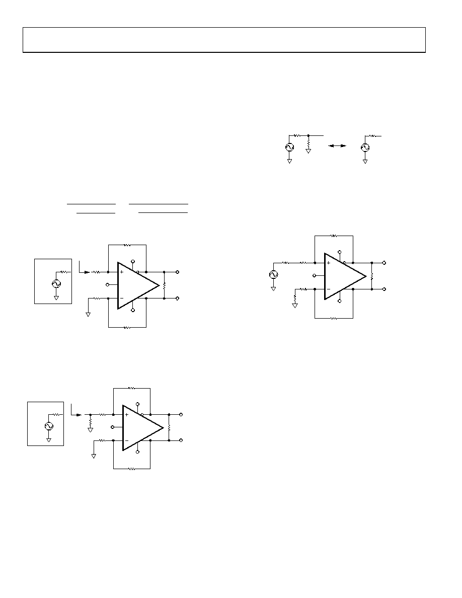
Terminating a Single-Ended Input
This section describes how to properly terminate a single-ended
499 . An example using an input source with a terminated output
voltage of 1 V p-p and source resistance of 50 illustrates the four
steps that must be followed. Note that because the terminated
output voltage of the source is 1 V p-p, the open-circuit output
voltage of the source is 2 V p-p. The source shown in Figure 59
indicates this open-circuit voltage.
1. The input impedance is calculated using the formula
Ω
665
)
499
(
2
499
1
499
)
(
2
1
,
=
+
×
=
+
×
=
F
G
F
G
se
IN
R
RS
50
VS
2V p-p
RIN, se
665
ADA4932-x
RL VOUT, dm
+VS
–VS
RG
499
RG
499
RF
499
RF
499
VOCM
07752-
050
Figure 59. Calculating Single-Ended Input Impedance, RIN
2. To match the 50 source resistance, calculate the
termination resistor, RT, using RT||665 = 50 . The
closest standard 1% value for RT is 53.6 .
ADA4932-x
RL
VOUT, dm
+VS
–VS
RS
50
RG
499
RG
499
RF
499
RF
499
VOCM
VS
2V p-p
RIN, se
50
RT
53.6
07752-
051
Figure 60. Adding Termination Resistor, RT
loop is now greater than the RG in the lower loop due to the
addition of the termination resistors. To compensate for the
imbalance of the gain resistors, add a correction resistor (RTS)
in series with RG in the lower loop. RTS is the Thevenin
equivalent of the source resistance, RS, and the termination
resistance, RT, and is equal to RS||RT.
RS
50
VS
2V p-p
RT
53.6
RTH
25.9
VTH
1.03V p-p
07752-
052
Figure 61. Calculating the Thevenin Equivalent
RTS = RTH = RS||RT = 25.9 . Note that VTH is greater than
1 V p-p, which was obtained with RT = 50 . The modified
circuit with the Thevenin equivalent (closest 1% value used for
RTH) of the terminated source and RTS in the lower feedback
loop is shown in Figure 62.
ADA4932-x
RL VOUT, dm
+VS
–VS
RTH
25.5
RG
499
RG
499
RF
499
RF
499
VOCM
VTH
1.03V p-p
RTS
25.5
07752-
053
Figure 62. Thevenin Equivalent and Matched Gain Resistors
Figure 62 presents a tractable circuit with matched
feedback loops that can be easily evaluated.
It is useful to point out two effects that occur with a termi-
nated input. The first is that the value of RG is increased in
both loops, lowering the overall closed-loop gain. The
second is that VTH is a little larger than 1 V p-p, as it would
be if RT = 50 . These two effects have opposite impacts on
the output voltage, and for large resistor values in the feedback
loops (~1 k), the effects essentially cancel each other out.
For small RF and RG, or high gains, however, the diminished
closed-loop gain is not canceled completely by the increased
The desired differential output in this example is 1 V p-p
because the terminated input signal was 1 V p-p and the
closed-loop gain = 1. The actual differential output voltage,
however, is equal to (1.03 V p-p)(499/524.5) = 0.98 V p-p.
To obtain the desired output voltage of 1 V p-p, a final gain
adjustment can be made by increasing RF without modifying
any of the input circuitry. This is discussed in Step 4.
Rev. C | Page 22 of 28
相关PDF资料 |
PDF描述 |
|---|---|
| ADA4939-2YCPZ-R7 | IC AMP DIFF DUAL ULDIST 24LFCSP |
| ADA4940-1ARZ-R7 | IC DIFF ADC DVR 18BIT LN 8SOIC |
| ADA4950-1YCPZ-RL | IC AMP DIFF LP 114MA 16LFCSP |
| ADEL2020ARZ-20-RL | IC OPAMP CF LN LP 60MA 20SOIC |
| ADL5561ACPZ-R7 | IC AMP DIFF RF/IF 2.9GHZ 16LFCSP |
相关代理商/技术参数 |
参数描述 |
|---|---|
| ADA4932-1YCPZ-RL1 | 制造商:AD 制造商全称:Analog Devices 功能描述:Low Power Differential ADC Driver |
| ADA4932-2 | 制造商:AD 制造商全称:Analog Devices 功能描述:Low Power Differential ADC Driver |
| ADA4932-2YCP-EBZ | 功能描述:BOARD EVAL FOR ADA4932-2YCP RoHS:是 类别:编程器,开发系统 >> 评估板 - 运算放大器 系列:- 产品培训模块:Lead (SnPb) Finish for COTS Obsolescence Mitigation Program 标准包装:1 系列:- |
| ADA4932-2YCPZ-R2 | 功能描述:IC AMP DIFF DUAL LP 80MA 24LFCSP RoHS:是 类别:集成电路 (IC) >> Linear - Amplifiers - Instrumentation 系列:- 标准包装:1,000 系列:- 放大器类型:电压反馈 电路数:4 输出类型:满摆幅 转换速率:33 V/µs 增益带宽积:20MHz -3db带宽:30MHz 电流 - 输入偏压:2nA 电压 - 输入偏移:3000µV 电流 - 电源:2.5mA 电流 - 输出 / 通道:30mA 电压 - 电源,单路/双路(±):4.5 V ~ 16.5 V,±2.25 V ~ 8.25 V 工作温度:-40°C ~ 85°C 安装类型:表面贴装 封装/外壳:14-SOIC(0.154",3.90mm 宽) 供应商设备封装:14-SOIC 包装:带卷 (TR) |
| ADA4932-2YCPZ-R2 | 制造商:Analog Devices 功能描述:IC DIFF AMP 560MHZ 2800V/ LFCSP-16 |
发布紧急采购,3分钟左右您将得到回复。