参数资料
| 型号: | ADA4938-1ACPZ-RL |
| 厂商: | Analog Devices Inc |
| 文件页数: | 13/28页 |
| 文件大小: | 0K |
| 描述: | IC ADC DRIVER DIFF 16-LFCSP |
| 标准包装: | 5,000 |
| 类型: | ADC 驱动器 |
| 应用: | 数据采集 |
| 安装类型: | 表面贴装 |
| 封装/外壳: | 16-VFQFN 裸露焊盘,CSP |
| 供应商设备封装: | 16-LFCSP-VQ |
| 包装: | 带卷 (TR) |
第1页第2页第3页第4页第5页第6页第7页第8页第9页第10页第11页第12页当前第13页第14页第15页第16页第17页第18页第19页第20页第21页第22页第23页第24页第25页第26页第27页第28页
ADA4938-1/ADA4938-2
Rev. A | Page 20 of 28
)
Similar to the case of a conventional op amp, the output noise
voltage densities can be estimated by multiplying the input-
referred terms at +IN and IN by the appropriate output factor,
where:
(
2
1
N
β
G
+
=
2
is the circuit noise gain.
G1
F1
G1
1
R
β
+
=
and
G2
F2
G2
2
R
β
+
=
are the feedback factors.
When RF1/RG1 = RF2/RG2, β1 = β2 = β, and the noise gain
becomes
G
F
N
R
β
G
+
=
1
Note that the output noise from VOCM goes to zero in this case.
The total differential output noise density, vnOD, is the root-sum-
square of the individual output noise terms.
∑
=
8
1
i
2
nOi
nOD
v
THE IMPACT OF MISMATCHES IN THE FEEDBACK
NETWORKS
As previously mentioned, even if the external feedback networks
(RF/RG) are mismatched, the internal common-mode feedback
loop still forces the outputs to remain balanced. The amplitudes
of the signals at each output remain equal and 180° out of phase.
The input-to-output, differential mode gain varies proportionately
to the feedback mismatch, but the output balance is unaffected.
As well as causing a noise contribution from VOCM, ratio matching
errors in the external resistors result in a degradation of the
ability of the circuit to reject input common-mode signals, much
the same as for a four-resistor difference amplifier made from a
conventional op amp.
In addition, if the dc levels of the input and output common-
mode voltages are different, matching errors result in a small
differential-mode output offset voltage. When G = +1, with a
ground referenced input signal and the output common-mode
level set to 2.5 V, an output offset of as much as 25 mV (1% of
the difference in common-mode levels) can result if 1% tolerance
resistors are used. Resistors of 1% tolerance result in a worst-case
input CMRR of about 40 dB, a worst-case differential-mode
output offset of 25 mV due to 2.5 V level-shift, and no significant
degradation in output balance error.
CALCULATING THE INPUT IMPEDANCE OF AN
APPLICATION CIRCUIT
The effective input impedance of a circuit depends on whether
the amplifier is being driven by a single-ended or differential
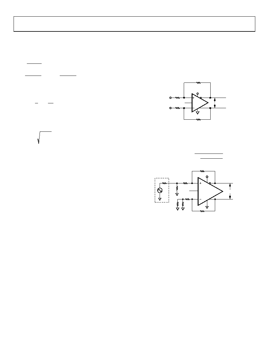
signal source. For balanced differential input signals, as shown
(+DIN and DIN) is simply RIN, dm = 2 × RG.
+VS
ADA4938
+IN
–IN
RF
+DIN
–DIN
VOCM
RG
VOUT, dm
06
59
2-
0
06
Figure 59. ADA4938 Configured for Balanced (Differential) Inputs
For an unbalanced, single-ended input signal (see Figure 60),
the input impedance is
()
+
×
=
F
G
F
G
cm
IN
R
2
1
,
RT
RS
ADA4938
+VS
RF
RG
RS
RG
RF
VOCM
RT
VOUT, dm
06
59
2-
00
7
Figure 60. ADA4938-x Configured for Unbalanced (Single-Ended) Input
The input impedance of the circuit is effectively higher than it
would be for a conventional op amp connected as an inverter
because a fraction of the differential output voltage appears at
the inputs as a common-mode signal, partially bootstrapping
the voltage across the Input Gain Resistor RG.
INPUT COMMON-MODE VOLTAGE RANGE IN
SINGLE-SUPPLY APPLICATIONS
The ADA4938 is optimized for level-shifting, ground-referenced
input signals. As such, the center of the input common-mode
range is shifted approximately 1 V down from midsupply. The
input common-mode range at the summing nodes of the amplifier
is from 0.3 V above VS to 1.6 V below +VS. To avoid clipping at
the outputs, the voltage swing at the +IN and IN terminals must
be confined to these ranges.
相关PDF资料 |
PDF描述 |
|---|---|
| VI-2TV-MW-B1 | CONVERTER MOD DC/DC 5.8V 100W |
| AD7398BRU-REEL7 | IC DAC 12BIT QUAD SRL 16-TSSOP |
| ADA4937-1YCPZ-RL | IC ADC DIFF DRIVER 16-LFCSP |
| VE-24N-IV-F1 | CONVERTER MOD DC/DC 18.5V 150W |
| LTC6404IUD-4#TRPBF | IC AMP/DRIVER DIFF 16-QFN |
相关代理商/技术参数 |
参数描述 |
|---|---|
| ADA4938-1YCP-EBZ | 功能描述:BOARD EVAL FOR ADA4938-1YCP RoHS:是 类别:编程器,开发系统 >> 评估板 - 运算放大器 系列:- 产品培训模块:Lead (SnPb) Finish for COTS Obsolescence Mitigation Program 标准包装:1 系列:- |
| ADA4938-1YCPZ-R2 | 制造商:AD 制造商全称:Analog Devices 功能描述:Ultra-Low Distortion Differential ADC Driver |
| ADA4938-1YCPZ-R7 | 制造商:AD 制造商全称:Analog Devices 功能描述:Ultra-Low Distortion Differential ADC Driver |
| ADA4938-1YCPZ-RL | 制造商:AD 制造商全称:Analog Devices 功能描述:Ultra-Low Distortion Differential ADC Driver |
| ADA4938-2ACP-EBZ | 功能描述:24-LFCSP Package 2 - Dual Channels per IC Differential Amplifier Evaluation Board 制造商:analog devices inc. 系列:- 零件状态:过期 每 IC 通道数:2 - 双 放大器类型:差分 输出类型:差分 压摆率:- -3db 带宽:- 电流 - 输出/通道:- 工作温度:- 电流 - 电源(主 IC):- 电压 - 电源,单/双(±):- 板类型:裸(未填充) 所含物品:板 使用的 IC/零件:24-LFCSP 封装 标准包装:1 |
发布紧急采购,3分钟左右您将得到回复。