参数资料
| 型号: | ADA4938-1ACPZ-RL |
| 厂商: | Analog Devices Inc |
| 文件页数: | 16/28页 |
| 文件大小: | 0K |
| 描述: | IC ADC DRIVER DIFF 16-LFCSP |
| 标准包装: | 5,000 |
| 类型: | ADC 驱动器 |
| 应用: | 数据采集 |
| 安装类型: | 表面贴装 |
| 封装/外壳: | 16-VFQFN 裸露焊盘,CSP |
| 供应商设备封装: | 16-LFCSP-VQ |
| 包装: | 带卷 (TR) |
第1页第2页第3页第4页第5页第6页第7页第8页第9页第10页第11页第12页第13页第14页第15页当前第16页第17页第18页第19页第20页第21页第22页第23页第24页第25页第26页第27页第28页
ADA4938-1/ADA4938-2
Rev. A | Page 23 of 28
LAYOUT, GROUNDING, AND BYPASSING
As a high speed device, the ADA4938-x is sensitive to the
PCB environment in which it operates. Realizing its superior
performance requires attention to the details of high speed
PCB design.
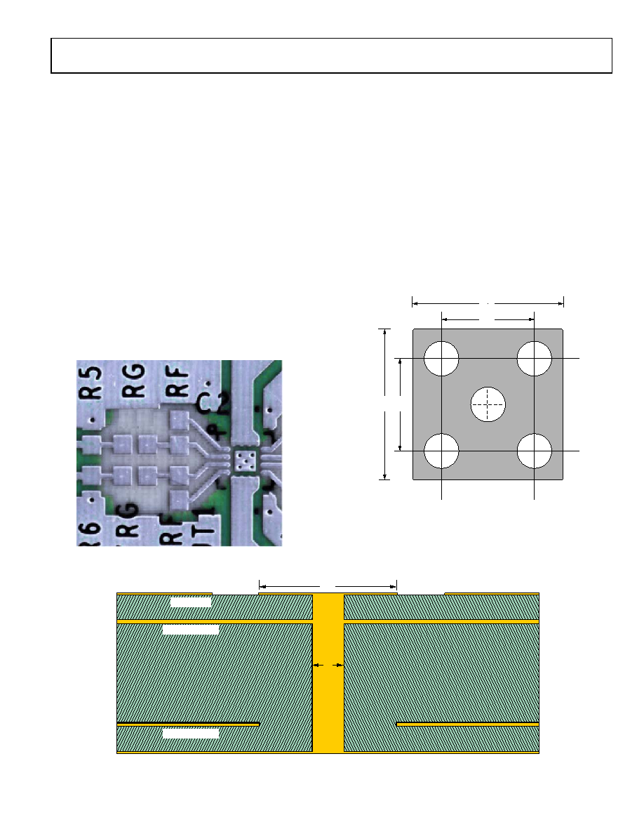
The first requirement is a solid ground plane that covers as much of
the board area around the ADA4938-x as possible. However, the
area near the feedback resistors (RF), input gain resistors (RG),
and the input summing nodes should be cleared of all ground
and power planes (see Figure 66). Clearing the ground and
power planes minimizes any stray capacitance at these nodes
and prevents peaking of the response of the amplifier at high
frequencies.
The thermal resistance, θJA, is specified for the device, including
the exposed pad, soldered to a high thermal conductivity 4-layer
circuit board, as described in EIA/JESD 51-7. The exposed pad
is electrically isolated from the device; therefore, it can be con-
nected to a ground plane using vias. Examples of the thermal
attach pad and via structure for the ADA4938-1 are shown in
06
59
2-
00
8
Figure 66. Ground and Power Plane Voiding in Vicinity of RF and RG
Bypass the power supply pins as close to the device as possible
and directly to a nearby ground plane. Use high frequency ceramic
chip capacitors. It is recommended that two parallel bypass capa-
citors (1000 pF and 0.1 μF) be used for each supply with the
1000 pF capacitor placed closer to the device; if further away,
provide low frequency bypassing using 10 μF tantalum capacitors
from each supply to ground.
Signal routing should be short and direct to avoid parasitic
effects. Wherever complementary signals exist, provide a
symmetrical layout to maximize balanced performance.
When routing differential signals over a long distance, keep
PCB traces close together and twist any differential wiring to
minimize loop area. Doing this reduces radiated energy and
makes the circuit less susceptible to interference.
06
59
2-
0
60
1.30
0.80
1.30
Figure 67. Recommended PCB Thermal Attach Pad (ADA4938-1)
(Dimensions in mm)
06
59
2-
06
1
0.30
PLATED
VIA HOLE
1.30
GROUND PLANE
POWER PLANE
BOTTOM METAL
TOP METAL
Figure 68. Cross-Section of a 4-Layer PCB (ADA4938-1) Showing a Thermal Via Connection to the Buried Ground Plane (Dimensions in mm)
相关PDF资料 |
PDF描述 |
|---|---|
| VI-2TV-MW-B1 | CONVERTER MOD DC/DC 5.8V 100W |
| AD7398BRU-REEL7 | IC DAC 12BIT QUAD SRL 16-TSSOP |
| ADA4937-1YCPZ-RL | IC ADC DIFF DRIVER 16-LFCSP |
| VE-24N-IV-F1 | CONVERTER MOD DC/DC 18.5V 150W |
| LTC6404IUD-4#TRPBF | IC AMP/DRIVER DIFF 16-QFN |
相关代理商/技术参数 |
参数描述 |
|---|---|
| ADA4938-1YCP-EBZ | 功能描述:BOARD EVAL FOR ADA4938-1YCP RoHS:是 类别:编程器,开发系统 >> 评估板 - 运算放大器 系列:- 产品培训模块:Lead (SnPb) Finish for COTS Obsolescence Mitigation Program 标准包装:1 系列:- |
| ADA4938-1YCPZ-R2 | 制造商:AD 制造商全称:Analog Devices 功能描述:Ultra-Low Distortion Differential ADC Driver |
| ADA4938-1YCPZ-R7 | 制造商:AD 制造商全称:Analog Devices 功能描述:Ultra-Low Distortion Differential ADC Driver |
| ADA4938-1YCPZ-RL | 制造商:AD 制造商全称:Analog Devices 功能描述:Ultra-Low Distortion Differential ADC Driver |
| ADA4938-2ACP-EBZ | 功能描述:24-LFCSP Package 2 - Dual Channels per IC Differential Amplifier Evaluation Board 制造商:analog devices inc. 系列:- 零件状态:过期 每 IC 通道数:2 - 双 放大器类型:差分 输出类型:差分 压摆率:- -3db 带宽:- 电流 - 输出/通道:- 工作温度:- 电流 - 电源(主 IC):- 电压 - 电源,单/双(±):- 板类型:裸(未填充) 所含物品:板 使用的 IC/零件:24-LFCSP 封装 标准包装:1 |
发布紧急采购,3分钟左右您将得到回复。