- 您现在的位置:买卖IC网 > PDF目录5953 > ADA4940-2ACPZ-RL (Analog Devices Inc)IC DIFF ADC DVR 18BIT LN 24LFCSP PDF资料下载
参数资料
| 型号: | ADA4940-2ACPZ-RL |
| 厂商: | Analog Devices Inc |
| 文件页数: | 18/33页 |
| 文件大小: | 0K |
| 描述: | IC DIFF ADC DVR 18BIT LN 24LFCSP |
| 标准包装: | 5,000 |
| 放大器类型: | 差分 |
| 电路数: | 2 |
| 输出类型: | 差分 |
| 转换速率: | 95 V/µs |
| -3db带宽: | 260MHz |
| 电流 - 输入偏压: | 1.1µA |
| 电压 - 输入偏移: | 60µV |
| 电流 - 电源: | 1.25mA |
| 电流 - 输出 / 通道: | 46mA |
| 电压 - 电源,单路/双路(±): | 3 V ~ 7 V |
| 工作温度: | -40°C ~ 125°C |
| 安装类型: | 表面贴装 |
| 封装/外壳: | 24-VFQFN 裸露焊盘,CSP |
| 供应商设备封装: | 24-LFCSP-VQ(4x4) |
| 包装: | 带卷 (TR) |
第1页第2页第3页第4页第5页第6页第7页第8页第9页第10页第11页第12页第13页第14页第15页第16页第17页当前第18页第19页第20页第21页第22页第23页第24页第25页第26页第27页第28页第29页第30页第31页第32页第33页
ADA4940-1/ADA4940-2
Data Sheet
Rev. C | Page 24 of 32
Table 15 and Table 16 list several common gain settings, recommended resistor values, input impedances, and output noise density for both
balanced and unbalanced input configurations.
Nominal Gain (dB)
RF (Ω)
RG (Ω)
RIN, dm (Ω)
Differential Output Noise Density (nV/√Hz)
RTI (nV/√Hz)
0
1000
2000
11.3
6
1000
500
1000
15.4
7.7
10
1000
318
636
20.0
6.8
14
1000
196
392
27.7
5.5
Nominal Gain (dB)
RF (Ω)
RG (Ω)
RT (Ω)
RIN,se (Ω)
RG1 (Ω)1
Differential Output Noise Density (nV/√Hz)
RTI (nV/√Hz)
0
1000
52.3
1333
1025
11.2
6
1000
500
53.6
750
526
15.0
7.5
10
1000
318
54.9
512
344
19.0
6.3
14
1000
196
59.0
337
223
25.3
5
1 RG1 = RG + (RS||RT)
IMPACT OF MISMATCHES IN THE FEEDBACK
NETWORKS
Even if the external feedback networks (RF/RG) are mismatched,
the internal common-mode feedback loop still forces the outputs
to remain balanced. The amplitudes of the signals at each output
remain equal and 180° out of phase. The input-to-output,
differential mode gain varies proportionately to the feedback
mismatch, but the output balance is unaffected.
As well as causing a noise contribution from VOCM, ratio-matching
errors in the external resistors result in a degradation of the ability
of the circuit to reject input common-mode signals, much the
same as for a four resistors difference amplifier made from a
conventional op amp.
In addition, if the dc levels of the input and output common-
mode voltages are different, matching errors result in a small
differential mode, output offset voltage. When G = 1, with a
ground-referenced input signal and the output common-mode
level set to 2.5 V, an output offset of as much as 25 mV (1% of
the difference in common-mode levels) can result if 1% tolerance
resistors are used. Resistors of 1% tolerance result in a worst-
case input CMRR of about 40 dB, a worst-case differential mode
output offset of 25 mV due to the 2.5 V level-shift, and no
significant degradation in output balance error.
CALCULATING THE INPUT IMPEDANCE OF AN
APPLICATION CIRCUIT
The effective input impedance of a circuit depends on whether
the amplifier is being driven by a single-ended or differential
signal source. For balanced differential input signals, as shown
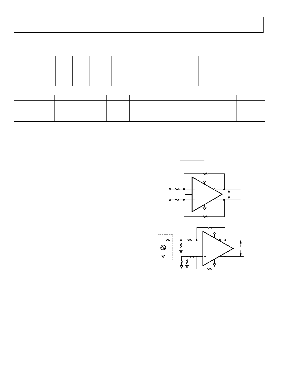
(+DIN and DIN) is simply RIN, dm = 2 × RG.
For an unbalanced, single-ended input signal (see Figure 65), the
input impedance is
F
G
F
G
se
IN
R
2
1
,
+VS
ADA4940-1/
ADA4940-2
+IN
–IN
RF
+DIN
–DIN
VOCM
RG
VOUT, dm
08
45
2-
05
1
Figure 64. ADA4940-1/ADA4940-2 Configured for Balanced (Differential) Inputs
RT
RS
ADA4940-1/
ADA4940-2
+VS
RF
RG
RS
RG
RF
VOCM
RT
VOUT, dm
08
452
-052
+IN
–IN
Figure 65. ADA4940-1/ADA4940-2 Configured for Unbalanced (Single-Ended)
Input
The input impedance of the circuit is effectively higher than it
would be for a conventional op amp connected as an inverter
because a fraction of the differential output voltage appears at
the inputs as a common-mode signal, partially bootstrapping
the voltage across the input resistor RG1.
相关PDF资料 |
PDF描述 |
|---|---|
| MCP621-E/SN | IC OPAMP SGL 2.5V R-R 8-SOIC |
| SMBJ7.5CAHE3/52 | TVS BIDIR 600W 7.5V 5% SMB |
| SMBJ7.0CAHE3/52 | TVS BIDIR 600W 7V 5% SMB |
| TSW-133-14-L-D | CONN HEADER 66POS .100" DL GOLD |
| SMBJ78CAHE3/52 | TVS BIDIR 600W 78V 5% SMB |
相关代理商/技术参数 |
参数描述 |
|---|---|
| ADA4941 | 制造商:AD 制造商全称:Analog Devices 功能描述:16-Bit, 100 kSPS PulSAR, Differential ADC in MSOP |
| ADA4941-1 | 制造商:AD 制造商全称:Analog Devices 功能描述:16-Bit Lower Power |
| ADA4941-1YCP-EBZ | 功能描述:BOARD EVAL FOR ADA4941-1YCP RoHS:是 类别:编程器,开发系统 >> 评估板 - 运算放大器 系列:- 产品培训模块:Lead (SnPb) Finish for COTS Obsolescence Mitigation Program 标准包装:1 系列:- |
| ADA4941-1YCPZ-R2 | 制造商:Analog Devices 功能描述:SP Amp DIFF Line Driver Amp Single R-R O/P 12V 8-Pin LFCSP EP T/R 制造商:Analog Devices 功能描述:SP Amp DIFF Line Driver Amp Single R-R O/P 12V 8-Pin LFCSP EP Tape & Reel |
| ADA4941-1YCPZ-R7 | 功能描述:IC AMP DIFF ADC DVR 18BIT 8LFCSP RoHS:是 类别:集成电路 (IC) >> 线性 - 放大器 - 专用 系列:- 产品培训模块:Lead (SnPb) Finish for COTS Obsolescence Mitigation Program 标准包装:60 系列:- 类型:可变增益放大器 应用:CATV 安装类型:表面贴装 封装/外壳:20-WQFN 裸露焊盘 供应商设备封装:20-TQFN-EP(5x5) 包装:托盘 |
发布紧急采购,3分钟左右您将得到回复。