- 您现在的位置:买卖IC网 > PDF目录2063 > ADA4941-1YRZ-R7 (Analog Devices Inc)IC DIFF ADC DRIVER 18BIT 8SOIC PDF资料下载
参数资料
| 型号: | ADA4941-1YRZ-R7 |
| 厂商: | Analog Devices Inc |
| 文件页数: | 23/25页 |
| 文件大小: | 0K |
| 描述: | IC DIFF ADC DRIVER 18BIT 8SOIC |
| 设计资源: | Converting a Single-Ended Signal with AD7982 Differential PulSAR ADC (CN0032) Converting a Single-Ended Signal with AD7984 Differential PulSAR ADC (CN0033) |
| 标准包装: | 1,000 |
| 类型: | ADC 驱动器 |
| 应用: | 数据采集 |
| 安装类型: | 表面贴装 |
| 封装/外壳: | 8-SOIC(0.154",3.90mm 宽) |
| 供应商设备封装: | 8-SO |
| 包装: | 带卷 (TR) |
ADA4941-1
Rev. C | Page 6 of 24
ABSOLUTE MAXIMUM RATINGS
Table 4.
Parameter
Rating
Supply Voltage
12 V
Power Dissipation
Storage Temperature Range
65°C to +125°C
Operating Temperature Range
40°C to +85°C
Lead Temperature (Soldering 10 sec)
300°C
Junction Temperature
150°C
Stresses above those listed under Absolute Maximum Ratings
may cause permanent damage to the device. This is a stress
rating only; functional operation of the device at these or any
other conditions above those indicated in the operational
section of this specification is not implied. Exposure to absolute
maximum rating conditions for extended periods may affect
device reliability.
THERMAL RESISTANCE
θJA is specified for the worst-case conditions, that is, θJA is
specified for a device soldered in the circuit board with its
exposed paddle soldered to a pad (if applicable) on the PCB
surface that is thermally connected to a copper plane, with zero
airflow.
Table 5. Thermal Resistance
Package Type
θJA
θJC
Unit
8-Lead SOIC on 4-Layer Board
126
28
°C/W
8-Lead LFCSP with EP on 4-Layer Board
83
19
°C/W
Maximum Power Dissipation
The maximum safe power dissipation in the ADA4941-1
package is limited by the associated rise in junction temperature
(TJ) on the die. At approximately 150°C, which is the glass
transition temperature, the plastic changes its properties. Even
temporarily exceeding this temperature limit can change the
stresses that the package exerts on the die, permanently shifting
the parametric performance of the ADA4941-1. Exceeding a
junction temperature of 150°C for an extended period can
result in changes in the silicon devices potentially causing
failure.
The power dissipated in the package (PD) is the sum of the
quiescent power dissipation and the power dissipated in the
package due to the load drive for all outputs. The quiescent
power is the voltage between the supply pins (VS) times the
quiescent current (IS). The power dissipated due to the load
drive depends upon the particular application. For each output,
the power due to load drive is calculated by multiplying the load
current by the associated voltage drop across the device. The
power dissipated due to all of the loads is equal to the sum of
the power dissipation due to each individual load. RMS voltages
and currents must be used in these calculations.
Airflow increases heat dissipation, effectively reducing θJA. In
addition, more metal directly in contact with the package leads
from metal traces, through holes, ground, and power planes
reduces the θJA. The exposed paddle on the underside of the
package must be soldered to a pad on the PCB surface that is
thermally connected to a copper plane to achieve the specified θJA.
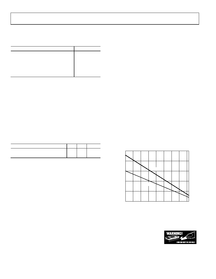
Figure 3 shows the maximum safe power dissipation in the
packages vs. the ambient temperature for the 8-lead SOIC
(126°C/W) and for the 8-lead LFCSP (83°C/W) on a JEDEC
standard 4-layer board. The LFCSP must have its underside
paddle soldered to a pad that is thermally connected to a PCB
plane. θJA values are approximations.
2.5
0
–40
120
AMBIENT TEMPERATURE (°C)
MA
XI
MU
M
PO
W
ER
D
ISSI
PA
T
IO
N
(W
)
2.0
1.5
1.0
0.5
–20
0
20
40
60
80
100
LFCSP
SOIC
05704-
002
Figure 3. Maximum Power Dissipation vs. Temperature for a 4-Layer Board
ESD CAUTION
ESD (electrostatic discharge) sensitive device. Electrostatic charges as high as 4000 V readily accumulate on
the human body and test equipment and can discharge without detection. Although this product features
proprietary ESD protection circuitry, permanent damage may occur on devices subjected to high energy
electrostatic discharges. Therefore, proper ESD precautions are recommended to avoid performance
degradation or loss of functionality.
相关PDF资料 |
PDF描述 |
|---|---|
| ADA4960-1ACPZ-R2 | IC ADC DRIVER DIFF 16LFCSP |
| ADATE205BSVZ | IC DCL DUAL 250MHZ ATE 100TQFP |
| ADATE206BSVZ | IC DCL DUAL 500MHZ ATE 100TQFP |
| ADAU1401AWBSTZ-RL | IC AUDIO PROC 28/56BIT 48LQFP |
| ADAU1401YSTZ-RL | IC AUDIO PROC 28/56BIT 48LQFP |
相关代理商/技术参数 |
参数描述 |
|---|---|
| ADA4941-1YRZ-RL | 功能描述:IC DIFF ADC DRIVER 18BIT 8SOIC RoHS:是 类别:集成电路 (IC) >> 线性 - 放大器 - 专用 系列:- 产品培训模块:Lead (SnPb) Finish for COTS Obsolescence Mitigation Program 标准包装:60 系列:- 类型:可变增益放大器 应用:CATV 安装类型:表面贴装 封装/外壳:20-WQFN 裸露焊盘 供应商设备封装:20-TQFN-EP(5x5) 包装:托盘 |
| ADA4950-1 | 制造商:AD 制造商全称:Analog Devices 功能描述:Low Power, Selectable Gain Differential ADC Driver, G = 1, 2, 3 |
| ADA4950-1YCP-EBZ | 功能描述:BOARD EVAL FOR ADA4950-1YCP RoHS:是 类别:编程器,开发系统 >> 评估板 - 运算放大器 系列:- 产品培训模块:Lead (SnPb) Finish for COTS Obsolescence Mitigation Program 标准包装:1 系列:- |
| ADA4950-1YCPZ-R2 | 制造商:Analog Devices 功能描述:SP Amp DIFF AMP Single ±5.5V/11V 16-Pin LFCSP EP T/R 制造商:Analog Devices 功能描述:FIXED GAIN 1,2&3 DIFF ADC DRIVER - Tape and Reel 制造商:Analog Devices 功能描述:SP Amp DIFF AMP Single }5.5V/11V 16-Pin LFCSP EP |
| ADA4950-1YCPZ-R7 | 功能描述:IC AMP DIFF LP 114MA 16LFCSP RoHS:是 类别:集成电路 (IC) >> Linear - Amplifiers - Instrumentation 系列:- 产品培训模块:Differential Circuit Design Techniques for Communication Applications 标准包装:1 系列:- 放大器类型:RF/IF 差分 电路数:1 输出类型:差分 转换速率:9800 V/µs 增益带宽积:- -3db带宽:2.9GHz 电流 - 输入偏压:3µA 电压 - 输入偏移:- 电流 - 电源:40mA 电流 - 输出 / 通道:- 电压 - 电源,单路/双路(±):3 V ~ 3.6 V 工作温度:-40°C ~ 85°C 安装类型:表面贴装 封装/外壳:16-VQFN 裸露焊盘,CSP 供应商设备封装:16-LFCSP-VQ 包装:剪切带 (CT) 产品目录页面:551 (CN2011-ZH PDF) 其它名称:ADL5561ACPZ-R7CT |
发布紧急采购,3分钟左右您将得到回复。