- 您现在的位置:买卖IC网 > PDF目录2063 > ADA4941-1YRZ-R7 (Analog Devices Inc)IC DIFF ADC DRIVER 18BIT 8SOIC PDF资料下载
参数资料
| 型号: | ADA4941-1YRZ-R7 |
| 厂商: | Analog Devices Inc |
| 文件页数: | 9/25页 |
| 文件大小: | 0K |
| 描述: | IC DIFF ADC DRIVER 18BIT 8SOIC |
| 设计资源: | Converting a Single-Ended Signal with AD7982 Differential PulSAR ADC (CN0032) Converting a Single-Ended Signal with AD7984 Differential PulSAR ADC (CN0033) |
| 标准包装: | 1,000 |
| 类型: | ADC 驱动器 |
| 应用: | 数据采集 |
| 安装类型: | 表面贴装 |
| 封装/外壳: | 8-SOIC(0.154",3.90mm 宽) |
| 供应商设备封装: | 8-SO |
| 包装: | 带卷 (TR) |
ADA4941-1
Rev. C | Page 16 of 24
In this case, the linear output voltage is limited by A1. On the
low end, the output of A1 starts to saturate and show degraded
linearity when VOP approaches 200 mV. On the high end, the
input of A1 becomes saturated and exhibits degraded linearity
when VIN moves beyond 4 V (within 1 V of VCC). This limits
the linear differential output voltage in the circuit shown in
Figure 49 to about 7.6 V p-p.
1k
1k
665
1.02k
402
500
A2
A1
REF
IN
2
8
4
5
FB
+5V
VS+
VS–
OUT+
+
–
VOP
1
3
OUT–
+
–
VON
VIN
+2.5V
6
05704-
055
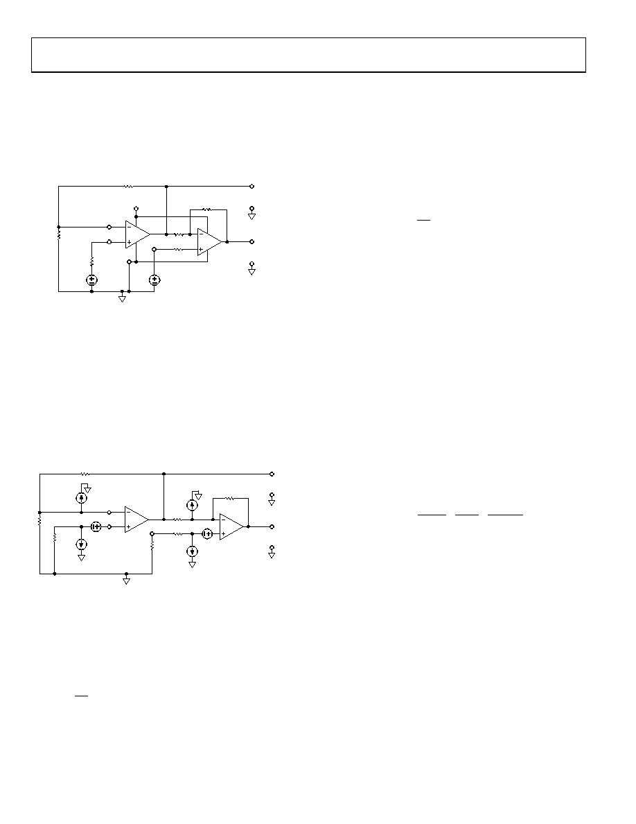
Figure 50. 5 V Supply, G = 5, Single-Ended-to-Differential Amplifier
Figure 50 shows a single 5 V supply connection for G = 5. The
RF and RG network sets the gain of A1 to 2.5, and the 2.5 V at
the REF input provides a centered 2.5 V output common-mode
voltage. The transfer function is then
VOP VON = 5(VIN) 5 V
(8)
The output range limits of A1 and A2 limit the differential
output voltage of the circuit shown in Figure 50 to approximately
8.4 V p-p.
DC ERROR CALCULATIONS
1k
1k
RG
RF
RS–IN
IBP–A2
IBN–A2
VOS–A1
500
A2
A1
REF
IN
2
8
4
5
FB
OUT+
+
–
VOP
1
OUT–
+
–
VON
VOS–A2
RS–REF
IBP–A1
IBN–A1
05704-
056
Figure 51. DC Error Sources
Figure 51 shows the major contributions to the dc output
voltage error. For each output, the total error voltage can be
calculated using familiar op amp concepts. Equation 9 expresses
the dc voltage error present at the VOP output.
[
]
F
BP
S
BP
OS
G
F
R
_A1
I
_IN
R
_A1
I
_A1
V
R
VOP_error
)
(
)
)(
(
1
+
+
=
(9)
When using data from the Specifications tables, it is often more
expedient to use input offset current in place of the individual
input bias currents when calculating errors. Input offset current
is defined as the magnitude of the difference between the two
input bias currents. Using this definition, each input bias
current can be expressed in terms of the average of the two
input bias currents, IB, and the input offset current, IOS, as
IBP, N = IB ± IOS/2. DC errors are minimized when RS = RF || RG. In
this case, Equation 9 is reduced to
[
]
)
||
(
)
(
1
G
F
S
F
OS
G
F
R
I
_A1
V
R
VOP_error
=
+
+
=
Equation 10 expresses the dc voltage error present at the VON
output.
VON_error = (VOP_error) + 2[VOS_A2
(IBP
_A2)(RS_REF + 500)] + 1000(IBN_A2)
(10)
The internal 500 resistor is provided on-chip to minimize dc
errors due to the input offset current in A2. The minimum
error is achieved when RS_REF = 0 . In this case, Equation 10
is reduced to
VON_error =
(VOP_error) + 2[VOS
_A2] + (IOS)1000
(RS_REF = 0 )
The differential output voltage error VO_error, dm, is the
difference between VOP_error and VON_error:
VO_error, dm = VOP_error VON_error
(11)
The output offset voltage of each amplifier in the ADA4941-1
also includes the effects of finite common-mode rejection ratio
(CMRR), power supply rejection ratio (PSRR), and dc open-
loop gain (AVOL).
VOL
S
CM
OS
A
VOUT
PSRR
V
CMRR
V
_nom
V
Δ
+
=
(12)
where:
VOS_nom is the nominal output offset voltage without including
the effects of CMRR, PSRR, and AVOL.
Δ indicates the change in conditions from nominal.
VCM is the input common-mode voltage (for A1, the voltage at
IN, and for A2, the voltage at REF).
VS is the power supply voltage.
VOUT is either op amp output.
相关PDF资料 |
PDF描述 |
|---|---|
| ADA4960-1ACPZ-R2 | IC ADC DRIVER DIFF 16LFCSP |
| ADATE205BSVZ | IC DCL DUAL 250MHZ ATE 100TQFP |
| ADATE206BSVZ | IC DCL DUAL 500MHZ ATE 100TQFP |
| ADAU1401AWBSTZ-RL | IC AUDIO PROC 28/56BIT 48LQFP |
| ADAU1401YSTZ-RL | IC AUDIO PROC 28/56BIT 48LQFP |
相关代理商/技术参数 |
参数描述 |
|---|---|
| ADA4941-1YRZ-RL | 功能描述:IC DIFF ADC DRIVER 18BIT 8SOIC RoHS:是 类别:集成电路 (IC) >> 线性 - 放大器 - 专用 系列:- 产品培训模块:Lead (SnPb) Finish for COTS Obsolescence Mitigation Program 标准包装:60 系列:- 类型:可变增益放大器 应用:CATV 安装类型:表面贴装 封装/外壳:20-WQFN 裸露焊盘 供应商设备封装:20-TQFN-EP(5x5) 包装:托盘 |
| ADA4950-1 | 制造商:AD 制造商全称:Analog Devices 功能描述:Low Power, Selectable Gain Differential ADC Driver, G = 1, 2, 3 |
| ADA4950-1YCP-EBZ | 功能描述:BOARD EVAL FOR ADA4950-1YCP RoHS:是 类别:编程器,开发系统 >> 评估板 - 运算放大器 系列:- 产品培训模块:Lead (SnPb) Finish for COTS Obsolescence Mitigation Program 标准包装:1 系列:- |
| ADA4950-1YCPZ-R2 | 制造商:Analog Devices 功能描述:SP Amp DIFF AMP Single ±5.5V/11V 16-Pin LFCSP EP T/R 制造商:Analog Devices 功能描述:FIXED GAIN 1,2&3 DIFF ADC DRIVER - Tape and Reel 制造商:Analog Devices 功能描述:SP Amp DIFF AMP Single }5.5V/11V 16-Pin LFCSP EP |
| ADA4950-1YCPZ-R7 | 功能描述:IC AMP DIFF LP 114MA 16LFCSP RoHS:是 类别:集成电路 (IC) >> Linear - Amplifiers - Instrumentation 系列:- 产品培训模块:Differential Circuit Design Techniques for Communication Applications 标准包装:1 系列:- 放大器类型:RF/IF 差分 电路数:1 输出类型:差分 转换速率:9800 V/µs 增益带宽积:- -3db带宽:2.9GHz 电流 - 输入偏压:3µA 电压 - 输入偏移:- 电流 - 电源:40mA 电流 - 输出 / 通道:- 电压 - 电源,单路/双路(±):3 V ~ 3.6 V 工作温度:-40°C ~ 85°C 安装类型:表面贴装 封装/外壳:16-VQFN 裸露焊盘,CSP 供应商设备封装:16-LFCSP-VQ 包装:剪切带 (CT) 产品目录页面:551 (CN2011-ZH PDF) 其它名称:ADL5561ACPZ-R7CT |
发布紧急采购,3分钟左右您将得到回复。