- 您现在的位置:买卖IC网 > PDF目录2139 > ADA4950-1YCPZ-RL (Analog Devices Inc)IC AMP DIFF LP 114MA 16LFCSP PDF资料下载
参数资料
| 型号: | ADA4950-1YCPZ-RL |
| 厂商: | Analog Devices Inc |
| 文件页数: | 11/28页 |
| 文件大小: | 0K |
| 描述: | IC AMP DIFF LP 114MA 16LFCSP |
| 标准包装: | 5,000 |
| 放大器类型: | 差分 |
| 电路数: | 1 |
| 输出类型: | 差分 |
| 转换速率: | 2900 V/µs |
| -3db带宽: | 750MHz |
| 电压 - 输入偏移: | 200µV |
| 电流 - 电源: | 9.5mA |
| 电流 - 输出 / 通道: | 114mA |
| 电压 - 电源,单路/双路(±): | 3 V ~ 11 V,±1.5 V ~ 5.5 V |
| 工作温度: | -40°C ~ 105°C |
| 安装类型: | 表面贴装 |
| 封装/外壳: | 16-VFQFN 裸露焊盘,CSP |
| 供应商设备封装: | 16-LFCSP-VQ |
| 包装: | 带卷 (TR) |
第1页第2页第3页第4页第5页第6页第7页第8页第9页第10页当前第11页第12页第13页第14页第15页第16页第17页第18页第19页第20页第21页第22页第23页第24页第25页第26页第27页第28页
Data Sheet
ADA4950-1/ADA4950-2
Rev. A | Page 19 of 28
APPLICATIONS INFORMATION
ANALYZING AN APPLICATION CIRCUIT
The ADA4950-x uses high open-loop gain and negative feedback
to force its differential and common-mode output voltages in
such a way as to minimize the differential and common-mode
error voltages. The differential error voltage is defined as the
voltage between the differential inputs labeled +INx and INx
(see Figure 52). For most purposes, this voltage can be assumed
to be 0. Similarly, the difference between the actual output
common-mode voltage and the voltage applied to VOCM can
also be assumed to be 0. Starting from these principles, any
application circuit can be analyzed.
SELECTING THE CLOSED-LOOP GAIN
Using the approach described in the Analyzing an Application
can be determined by
G
F
dm
IN
dm
OUT
R
V
=
,
where the input resistors (RG) and the feedback resistors (RF) on
each side are equal.
For G = 1, the +INA and INA inputs are used, and the +INB
and INB inputs are left floating. The differential gain in this
case is calculated as follows:
1
500
=
=
G
F
R
G
For G = 2, the +INB and INB inputs are used, and the +INA
and INA inputs are left floating. The differential gain in this
case is calculated as follows:
2
250
500
=
=
G
F
R
G
For G = 3, the +INA and +INB inputs are connected together,
and the INA and INB inputs are connected together. The
differential gain in this case is calculated as follows:
3
250
||
500
=
=
G
F
R
G
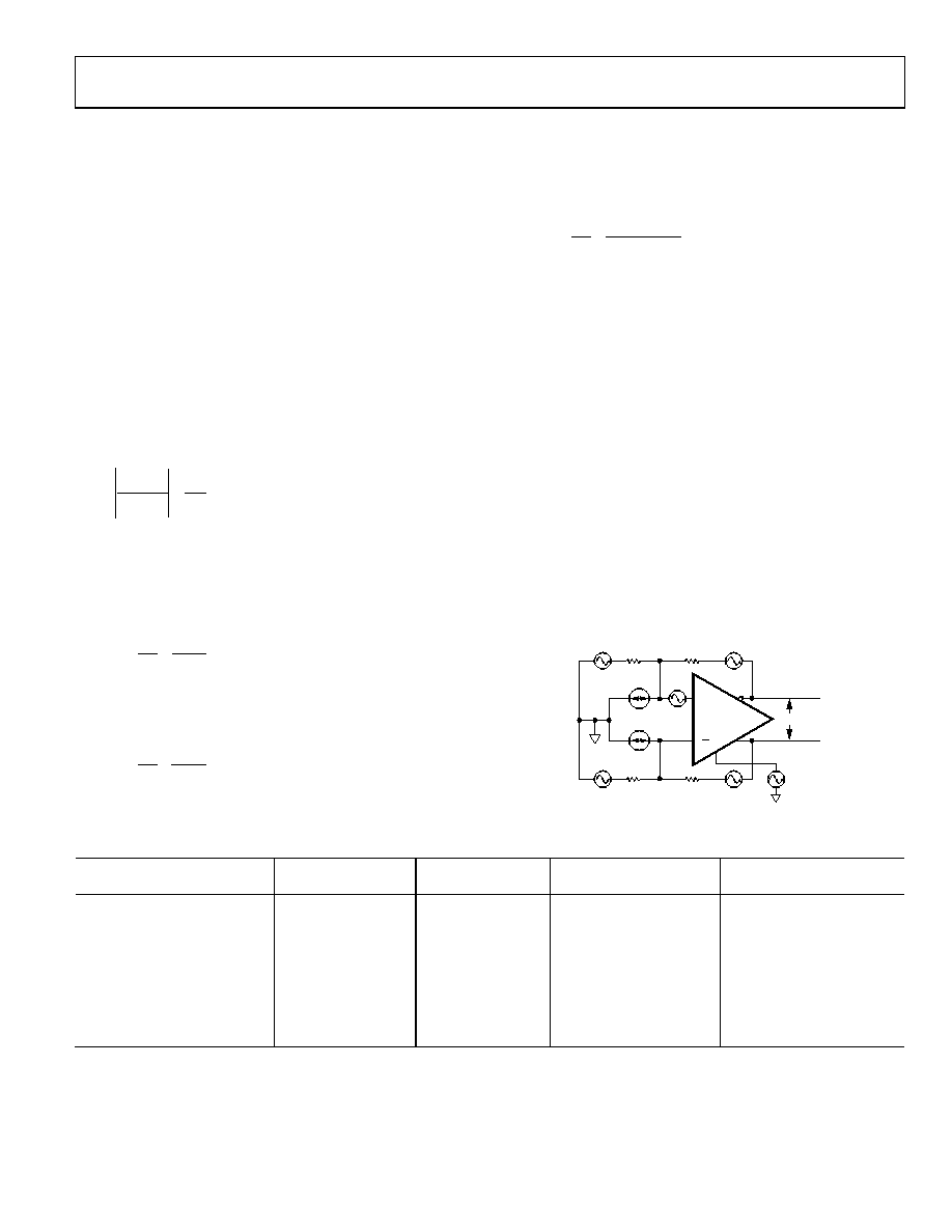
ESTIMATING THE OUTPUT NOISE VOLTAGE
The differential output noise of the ADA4950-x can be estimated
the selected gain. The input-referred noise voltage density, vnIN,
is modeled as a differential input, and the noise currents, inIN and
inIN+, appear between each input and ground. The output voltage
due to vnIN is obtained by multiplying vnIN by the noise gain, GN
currents are uncorrelated with the same mean-square value,
and each produces an output voltage that is equal to the noise
current multiplied by the associated feedback resistance. The
noise voltage density at the VOCM pin is vnCM. When the feedback
networks have the same feedback factor, as is true in most cases,
the output noise due to vnCM is common mode. Each of the four
resistors contributes (4kTRxx)1/2. The noise from the feedback
resistors appears directly at the output, and the noise from the
summarizes the input noise sources, the multiplication factors,
and the output-referred noise density terms.
ADA4950-x
+
RF2
vnOD
vnCM
VOCM
vnIN
RF1
RG2
RG1
vnRF1
vnRF2
vnRG1
vnRG2
inIN+
inIN–
07957-
053
Figure 53. Noise Model
Table 11. Output Noise Voltage Density Calculations for Matched Feedback Networks
Input Noise Contribution
Input Noise Term
Input Noise
Voltage Density
Output
Multiplication Factor
Differential Output Noise
Voltage Density Term
Differential Input
vnIN
GN
vnO1 = GN(vnIN)
Inverting Input
inIN
inIN × (RF2)
1
vnO2 = (inIN)(RF2)
Noninverting Input
inIN+
inIN+ × (RF1)
1
vnO3 = (inIN+)(RF1)
VOCM Input
vnCM
0
vnO4 = 0 V
Gain Resistor, RG1
vnRG1
(4kTRG1)1/2
RF1/RG1
vnO5 = (RF1/RG1)(4kTRG1)1/2
Gain Resistor, RG2
vnRG2
(4kTRG2)1/2
RF2/RG2
vnO6 = (RF2/RG2)(4kTRG2)1/2
Feedback Resistor, RF1
vnRF1
(4kTRF1)1/2
1
vnO7 = (4kTRF1)1/2
Feedback Resistor, RF2
vnRF2
(4kTRF2)1/2
1
vnO8 = (4kTRF2)1/2
相关PDF资料 |
PDF描述 |
|---|---|
| ADEL2020ARZ-20-RL | IC OPAMP CF LN LP 60MA 20SOIC |
| ADL5561ACPZ-R7 | IC AMP DIFF RF/IF 2.9GHZ 16LFCSP |
| ADL5562ACPZ-R7 | IC AMP DIFF RF/IF 3.3GHZ 16LFCSP |
| ADL5565ACPZ-R7 | IC AMP DIFF 6GHZ 16LFCSP |
| ADM4073TWRJZ-REEL7 | IC AMP CS 1.8MHZ SOT23-6 |
相关代理商/技术参数 |
参数描述 |
|---|---|
| ADA4950-2 | 制造商:AD 制造商全称:Analog Devices 功能描述:Low Power, Selectable Gain Differential ADC Driver, G = 1, 2, 3 |
| ADA4950-2YCP-EBZ | 功能描述:BOARD EVAL FOR ADA4950-2YCP RoHS:是 类别:编程器,开发系统 >> 评估板 - 运算放大器 系列:- 产品培训模块:Lead (SnPb) Finish for COTS Obsolescence Mitigation Program 标准包装:1 系列:- |
| ADA4950-2YCPZ-R2 | 制造商:Analog Devices 功能描述:SP Amp DIFF AMP Dual 制造商:Analog Devices 功能描述:FIXED GAIN 1,2&3 DIFF ADC DRIVER - Tape and Reel 制造商:Analog Devices 功能描述:SP Amp DIFF AMP Dual }5.5V/11V 24-Pin LFCSP EP |
| ADA4950-2YCPZ-R7 | 功能描述:IC AMP DIFF DUAL 114MA 24LFCSP RoHS:是 类别:集成电路 (IC) >> Linear - Amplifiers - Instrumentation 系列:- 标准包装:2,500 系列:- 放大器类型:通用 电路数:4 输出类型:- 转换速率:0.6 V/µs 增益带宽积:1MHz -3db带宽:- 电流 - 输入偏压:45nA 电压 - 输入偏移:2000µV 电流 - 电源:1.4mA 电流 - 输出 / 通道:40mA 电压 - 电源,单路/双路(±):3 V ~ 32 V,±1.5 V ~ 16 V 工作温度:0°C ~ 70°C 安装类型:表面贴装 封装/外壳:14-TSSOP(0.173",4.40mm 宽) 供应商设备封装:14-TSSOP 包装:带卷 (TR) 其它名称:LM324ADTBR2G-NDLM324ADTBR2GOSTR |
| ADA4950-2YCPZ-RL | 功能描述:IC AMP DIFF DUAL 114MA 24LFCSP RoHS:是 类别:集成电路 (IC) >> Linear - Amplifiers - Instrumentation 系列:- 标准包装:150 系列:- 放大器类型:音频 电路数:2 输出类型:- 转换速率:5 V/µs 增益带宽积:12MHz -3db带宽:- 电流 - 输入偏压:100nA 电压 - 输入偏移:500µV 电流 - 电源:6mA 电流 - 输出 / 通道:50mA 电压 - 电源,单路/双路(±):4 V ~ 32 V,±2 V ~ 16 V 工作温度:-40°C ~ 85°C 安装类型:表面贴装 封装/外壳:8-TSSOP(0.173",4.40mm 宽) 供应商设备封装:8-TSSOP 包装:管件 |
发布紧急采购,3分钟左右您将得到回复。