参数资料
| 型号: | ADADC80-Z-12 |
| 厂商: | Analog Devices Inc |
| 文件页数: | 2/16页 |
| 文件大小: | 0K |
| 描述: | IC ADC 12BIT INTEGRATED 32-CDIP |
| 标准包装: | 1 |
| 位数: | 12 |
| 采样率(每秒): | 40k |
| 数据接口: | 并联 |
| 转换器数目: | 1 |
| 功率耗散(最大): | 800mW |
| 电压电源: | 模拟和数字,双 ± |
| 工作温度: | -25°C ~ 85°C |
| 安装类型: | 通孔 |
| 封装/外壳: | 32-CDIP(0.910",23.12mm) |
| 供应商设备封装: | 32-CDIP 侧面铜焊 |
| 包装: | 管件 |
| 输入数目和类型: | 2 个单端,单极;2 个单端,双极 |
ADADC80
Rev. E | Page 10 of 16
Table 6. Input Voltage Range and LSB Values
Binary Output
Analog Input Voltage Range
Defined as
±10 V
±5 V
±2.5 V
0 V to +10 V
0 V to +5 V
Code Designation
COB1
COB1
or CTC2
or CTC2
CSB3
One Least Significant Bit (LSB)
FSR
20 V
10 V
5 V
10 V
5 V
2n
n = 8
78.13 mV
39.06 mV
19.53 mV
39.06 mV
19.53 mV
n = 10
19.53 mV
9.77 mV
4.88 mV
9.77 mV
4.88 mV
n = 12
4.88 mV
2.44 mV
1.22 mV
2.44 mV
1.22 mV
Transition Values
MSB
LSB
000. . . 0004
+Full scale
10 V 3/2 LSB
5 V 3/2 LSB
2.5 V 3/2 LSB
10 V 3/2 LSB
5 V 3/2 LSB
011. . . 111
Midscale
0
5 V
2.5 V
111. . . 110
Full scale
10 V + 1/2 LSB
5 V + 1/2 LSB
2.5 V + 1/2 LSB
0 V + 1/2 LSB
1 COB = complementary offset binary.
2 CTC = complementary twos complement; obtained by using the complement of the most significant bit (MSB). MSB is available on Pin 8.
3 CSB = complementary straight binary.
4 Voltages given are the nominal value for transition to the code specified.
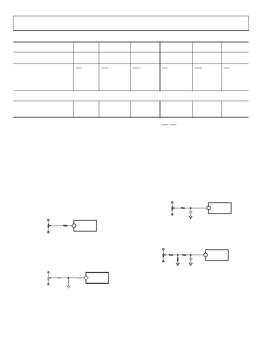
OFFSET ADJUSTMENT
The zero adjust circuit consists of a potentiometer connected
across ±VS with its slider connected through a 1.8 MΩ resistor
to COMPARATOR IN (Pin 11) for all ranges. As shown in
Figure 9, the tolerance of this fixed resistor is not critical, and a
carbon composition type is generally adequate. Using a carbon
composition resistor with a 1200 ppm/°C tempco contributes
a worst-case offset tempco of 8 × 244 × 106 × 1200 ppm/°C =
2.3 ppm/°C of FSR if the offset adjustment potentiometer is set
at either end of its adjustment range. Because the maximum
offset adjustment required is typically no more than ±4 LSB,
use of a carbon composition offset summing resistor typically
contributes no more than 1 ppm/°C of FSR offset tempco.
01
20
2-
0
09
ADADC80
1.8M
+15V
–15V
10k
TO
100k
11
COMPARATOR
IN
0
120
2-
010
Figure 9. Offset Adjustment Circuit
An alternative offset adjust circuit, which contributes negligible
offset tempco if metal film resistors (tempco < 100 ppm/°C) are
used, is shown in Figure 10. Note that the abbreviation MF in
Figure 10 and Figure 12 refer to metal film resistors.
ADADC80
180k
MF
180k
MF
22k
MF
+15V
–15V
10k
TO
100k
OFFSET
ADJUST
A
11
COMPARATOR
IN
0
120
2-
0
1
Figure 10. Low Tempco Zero Adjustment Circuit
In either zero adjust circuit, the fixed resistor connected to
COMPARATOR IN (Pin 11) should be located close to this pin
to keep the pin connection runs short. Pin 11 is quite sensitive
to external noise pickup.
GAIN ADJUSTMENT
The gain adjust circuit consists of a potentiometer connected
across ±VS with its slider connected through a 10 MΩ resistor
to the GAIN ADJUST (Pin 16), as shown in Figure 11.
ADADC80
10M
+15V
–15V
10k
TO
100k
GAIN
ADJUST
0.01F
16
GAIN
ADJUST
0
120
2-
0
12
Figure 11. Gain Adjustment Circuit
An alternative gain adjust circuit, which contributes negligible
gain tempco if metal film resistors (tempco < 100 ppm/°C) are
used, is shown in Figure 12.
ADADC80
270k
MF
270k
MF
+15V
–15V
10k
TO
100k
0.1F
6.8k
16
GAIN
ADJUST
Figure 12. Low Tempco Gain Adjustment Circuit
相关PDF资料 |
PDF描述 |
|---|---|
| ADATE207BBPZ | IC TIMING FORMATTER QUAD 256BGA |
| ADC0804LCN | IC ADC 8-BIT 10KSPS 1LSB 20-DIP |
| ADC0820CCM+ | IC ADC 8-BIT HS 20-SOIC |
| ADF4001BRU | IC CLOCK GEN PLL 16-TSSOP |
| ADF4002BRUZ-RL7 | IC PLL FREQUENCY SYNTH 16-TSSOP |
相关代理商/技术参数 |
参数描述 |
|---|---|
| ADADC80Z-12 | 制造商:AD 制造商全称:Analog Devices 功能描述:Analog-to-Digital Converter, 12-Bit |
| ADADC80Z-CBI-V | 制造商:Rochester Electronics LLC 功能描述:- Bulk 制造商:Analog Devices 功能描述: |
| adadc80z-ccd-i | 制造商:Rochester Electronics LLC 功能描述:- Bulk 制造商:Analog Devices 功能描述: |
| ADADC-816BD | 制造商:未知厂家 制造商全称:未知厂家 功能描述:Analog-to-Digital Converter, 10-Bit |
| ADADC-816KD | 制造商:未知厂家 制造商全称:未知厂家 功能描述:Analog-to-Digital Converter, 10-Bit |
发布紧急采购,3分钟左右您将得到回复。