参数资料
| 型号: | ADC0804LCN |
| 厂商: | Intersil |
| 文件页数: | 2/17页 |
| 文件大小: | 0K |
| 描述: | IC ADC 8-BIT 10KSPS 1LSB 20-DIP |
| 标准包装: | 1,080 |
| 位数: | 8 |
| 采样率(每秒): | 10k |
| 数据接口: | 并联 |
| 转换器数目: | 1 |
| 电压电源: | 单电源 |
| 工作温度: | 0°C ~ 70°C |
| 安装类型: | 通孔 |
| 封装/外壳: | 20-DIP(0.300",7.62mm) |
| 供应商设备封装: | 20-PDIP |
| 包装: | 管件 |
| 输入数目和类型: | 1 个差分,单极 |
| 其它名称: | ADC0804LCNIN ADC0804LCNIN-ND |
10
Such an adjusted reference voltage can accommodate a
reduced span or dynamic voltage range of the analog input
voltage. If the analog input voltage were to range from 0.5V to
3.5V, instead of 0V to 5V, the span would be 3V. With 0.5V
applied to the VlN(-) pin to absorb the offset, the reference
voltage can be made equal to 1/2 of the 3V span or 1.5V. The
A/D now will encode the VlN(+) signal from 0.5V to 3.5V with
the 0.5V input corresponding to zero and the 3.5V input
corresponding to full scale. The full 8 bits of resolution are
therefore applied over this reduced analog input voltage
range. The requisite connections are shown in Figure 13. For
expanded scale inputs, the circuits of Figures 14 and 15 can
be used.
Reference Accuracy Requirements
The converter can be operated in a pseudo-ratiometric mode
or an absolute mode. In ratiometric converter applications,
the magnitude of the reference voltage is a factor in both the
output of the source transducer and the output of the A/D
converter and therefore cancels out in the final digital output
code. In absolute conversion applicatIons, both the initial
value and the temperature stability of the reference voltage
are important accuracy factors in the operation of the A/D
converter. For VREF/2 voltages of 2.5V nominal value, initial
errors of
±10mV will cause conversion errors of ±1 LSB due
to the gain of 2 of the VREF/2 input. In reduced span
applications, the initial value and the stability of the VREF/2
input voltage become even more important. For example, if
the span is reduced to 2.5V, the analog input LSB voltage
value is correspondingly reduced from 20mV (5V span) to
10mV and 1 LSB at the VREF/2 input becomes 5mV. As can
be seen, this reduces the allowed initial tolerance of the
reference voltage and requires correspondingly less
absolute change with temperature variations. Note that
spans smaller than 2.5V place even tighter requirements on
the initial accuracy and stability of the reference source.
In general, the reference voltage will require an initial
adjustment. Errors due to an improper value of reference
voltage appear as full scale errors in the A/D transfer
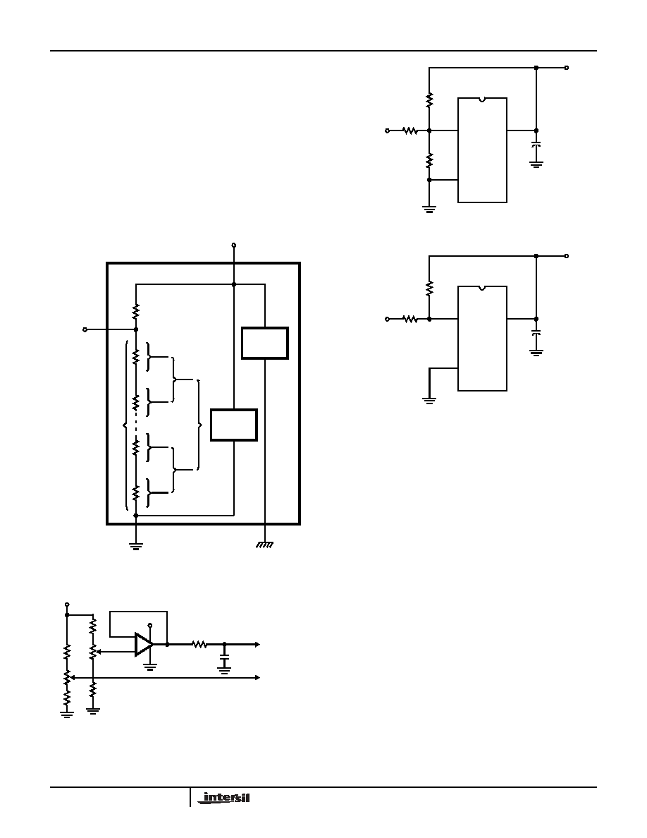
FIGURE 12. THE VREFERENCE DESIGN ON THE IC
FIGURE 13. OFFSETTING THE ZERO OF THE ADC080X AND
PERFORMING AN INPUT RANGE (SPAN)
ADJUSTMENT
V+
DGND
VREF/2
AGND
(VREF)
R
DIGITAL
CIRCUITS
ANALOG
CIRCUITS
9
810
20
DECODE
300
TO VREF/2
TO VIN(-)
ZERO SHIFT VOLTAGE
0.1
F
5V
-
+
VREF
(5V)
FS
ADJ.
“SPAN”/2
ICL7611
FIGURE 14. HANDLING
±10V ANALOG INPUT RANGE
FIGURE 15. HANDLING
±5V ANALOG INPUT RANGE
VIN(-)
2R
5V
2R
VIN ± 10V
R
VIN(+)
(VREF)
V+
20
10
F
6
7
+
ADC0803-
ADC0804
VIN(-)
R
5V
VIN ±5V
R
VIN(+)
(VREF)
V+
20
10
F
6
7
+
ADC0803-
ADC0804
ADC0803, ADC0804
相关PDF资料 |
PDF描述 |
|---|---|
| ADC0820CCM+ | IC ADC 8-BIT HS 20-SOIC |
| ADF4001BRU | IC CLOCK GEN PLL 16-TSSOP |
| ADF4002BRUZ-RL7 | IC PLL FREQUENCY SYNTH 16-TSSOP |
| ADF4007BCPZ-RL7 | IC DIVIDER/PLL SYNTHESZR 20LFCSP |
| ADF4106BRU | IC PLL FREQ SYNTHESIZER 16-TSSOP |
相关代理商/技术参数 |
参数描述 |
|---|---|
| ADC0804LCN | 制造商:Texas Instruments 功能描述:IC 8BIT ADC DIP20 804 |
| ADC0804LCN/A+ | 制造商:未知厂家 制造商全称:未知厂家 功能描述:Analog-to-Digital Converter, 8-Bit |
| ADC0804LCN/B+ | 制造商:未知厂家 制造商全称:未知厂家 功能描述:Analog-to-Digital Converter, 8-Bit |
| ADC0804LCN/NOPB | 功能描述:模数转换器 - ADC 8B UP COMPATIBLE ADC RoHS:否 制造商:Texas Instruments 通道数量:2 结构:Sigma-Delta 转换速率:125 SPs to 8 KSPs 分辨率:24 bit 输入类型:Differential 信噪比:107 dB 接口类型:SPI 工作电源电压:1.7 V to 3.6 V, 2.7 V to 5.25 V 最大工作温度:+ 85 C 安装风格:SMD/SMT 封装 / 箱体:VQFN-32 |
| ADC0804LCN/NOPB | 制造商:Texas Instruments 功能描述:A/D Converter (A-D) IC |
发布紧急采购,3分钟左右您将得到回复。