- 您现在的位置:买卖IC网 > PDF目录378277 > ADC0805LCN (NATIONAL SEMICONDUCTOR CORP) 8-Bit uP Compatible A/D Converters PDF资料下载
参数资料
| 型号: | ADC0805LCN |
| 厂商: | NATIONAL SEMICONDUCTOR CORP |
| 元件分类: | ADC |
| 英文描述: | 8-Bit uP Compatible A/D Converters |
| 中文描述: | 1-CH 8-BIT SUCCESSIVE APPROXIMATION ADC, PARALLEL ACCESS, PDIP20 |
| 封装: | PLASTIC, DIP-20 |
| 文件页数: | 29/41页 |
| 文件大小: | 1118K |
| 代理商: | ADC0805LCN |
第1页第2页第3页第4页第5页第6页第7页第8页第9页第10页第11页第12页第13页第14页第15页第16页第17页第18页第19页第20页第21页第22页第23页第24页第25页第26页第27页第28页当前第29页第30页第31页第32页第33页第34页第35页第36页第37页第38页第39页第40页第41页
Functional Description
(Continued)
ing I/O input instructions. For example, MUX channel selec-
tion for the A/D can be accomplished with this operating
mode.
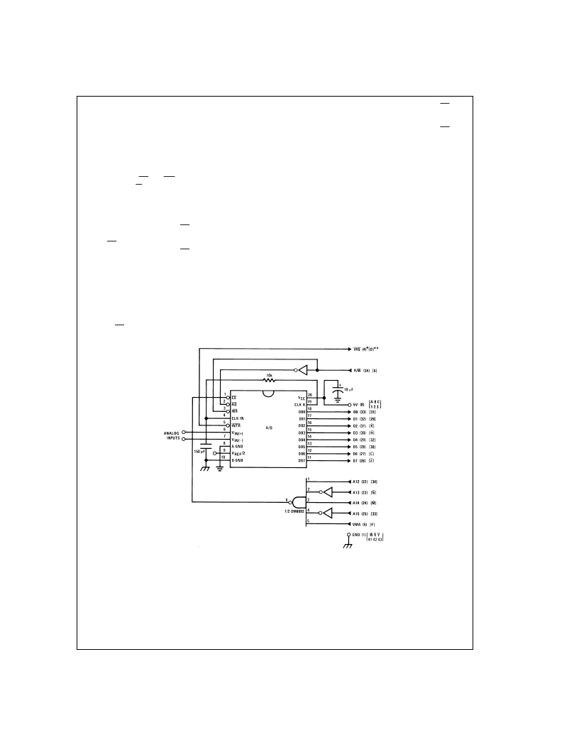
4.3 Interfacing 6800 Microprocessor Derivatives
(6502, etc.)
The control bus for the 6800 microprocessor derivatives
does not use the RD and WR strobe signals. Instead it em-
ploys a single R/W line and additional timing, if needed, can
be derived fom the
φ
2 clock. All I/O devices are memory
mapped in the 6800 system, and a special signal, VMA, indi-
cates that the current address is valid. Figure 15 shows an
interface schematic where the A/D is memory mapped in the
6800 system. For simplicity, the CS decoding is shown using
1
2
DM8092. Note that in many 6800 systems, an already de-
coded 4/5 line is brought out to the common bus at pin 21.
This can be tied directly to the CS pin of the A/D, provided
that no other devices are addressed at HX ADDR: 4XXX or
5XXX.
The following subroutine performs essentially the same func-
tion as in the case of the 8080Ainterface and it can be called
from anywhere in the user’s program.
In Figure 16 the ADC0801 series is interfaced to the M6800
microprocessor through (the arbitrarily chosen) Port B of the
MC6820 or MC6821 Peripheral Interface Adapter, (PIA).
Here the CS pin of the A/D is grounded since the PIA is al-
ready memory mapped in the M6800 system and no CS de-
coding is necessary. Also notice that the A/D output data
lines are connected to the microprocessor bus under pro-
gram control through the PIA and therefore the A/D RD pin
can be grounded.
Asample interface program equivalent to the previous one is
shown below Figure 16 The PIA Data and Control Registers
of Port B are located at HEX addresses 8006 and 8007, re-
spectively.
5.0 GENERAL APPLICATIONS
The following applications show some interesting uses for
the A/D. The fact that one particular microprocessor is used
is not meant to be restrictive. Each of these application cir-
cuits would have its counterpart using any microprocessor
that is desired.
5.1 Multiple ADC0801 Series to MC6800 CPU Interface
To transfer analog data from several channels to a single mi-
croprocessor system, a multiple converter scheme presents
several advantages over the conventional multiplexer
single-converter approach. With theADC0801 series, the dif-
ferential inputs allow individual span adjustment for each
channel. Furthermore, all analog input channels are sensed
simultaneously, which essentially divides the microproces-
sor’s total system servicing time by the number of channels,
since all conversions occur simultaneously. This scheme is
shown in Figure 17
DS005671-24
Note 20:
Numbers in parentheses refer to MC6800 CPU pin out.
Note 21:
Number or letters in brackets refer to standard M6800 system common bus code.
FIGURE 15. ADC0801-MC6800 CPU Interface
A
www.national.com
29
相关PDF资料 |
PDF描述 |
|---|---|
| ADC0801 | 8-Bit uP Compatible A/D Converters |
| ADC0802 | 8-Bit uP Compatible A/D Converters |
| ADC0802LCN | 8-Bit uP Compatible A/D Converters |
| ADC0805 | 8-Bit uP Compatible A/D Converters |
| ADC0802LCWM | 8-Bit uP Compatible A/D Converters |
相关代理商/技术参数 |
参数描述 |
|---|---|
| ADC0805LCN/A+ | 制造商:未知厂家 制造商全称:未知厂家 功能描述:Analog-to-Digital Converter, 8-Bit |
| ADC0805LCN/B+ | 制造商:未知厂家 制造商全称:未知厂家 功能描述:Analog-to-Digital Converter, 8-Bit |
| ADC0805LCN/NOPB | 功能描述:IC ADC 8BIT MPU COMPAT 20-DIP RoHS:是 类别:集成电路 (IC) >> 数据采集 - 模数转换器 系列:- 产品培训模块:Lead (SnPb) Finish for COTS Obsolescence Mitigation Program 标准包装:2,500 系列:- 位数:12 采样率(每秒):3M 数据接口:- 转换器数目:- 功率耗散(最大):- 电压电源:- 工作温度:- 安装类型:表面贴装 封装/外壳:SOT-23-6 供应商设备封装:SOT-23-6 包装:带卷 (TR) 输入数目和类型:- |
| ADC0806 | 制造商:NSC 制造商全称:National Semiconductor 功能描述:8-Bit, 20 MSPS to 60 MSPS, 1.3 mW/MSPS A/D Converter |
| ADC08060 | 制造商:NSC 制造商全称:National Semiconductor 功能描述:8-Bit, 20 MSPS to 60 MSPS, 1.3 mW/MSPS A/D Converter |
发布紧急采购,3分钟左右您将得到回复。