- 您现在的位置:买卖IC网 > PDF目录378277 > ADC08061BIN (NATIONAL SEMICONDUCTOR CORP) TIMER DIGITAL LED RoHS Compliant: Yes PDF资料下载
参数资料
| 型号: | ADC08061BIN |
| 厂商: | NATIONAL SEMICONDUCTOR CORP |
| 元件分类: | ADC |
| 英文描述: | TIMER DIGITAL LED RoHS Compliant: Yes |
| 中文描述: | 1-CH 8-BIT FLASH METHOD ADC, PARALLEL ACCESS, DIP20 |
| 封装: | DIP-20 |
| 文件页数: | 5/16页 |
| 文件大小: | 307K |
| 代理商: | ADC08061BIN |
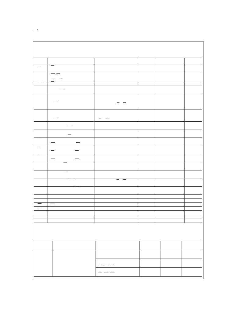
AC Electrical Characteristics
(Continued)
The following specifications apply for V
+
= 5V, t
= t
= 10 ns, V
REF+
= 5V, V
REF
= 0V unless otherwise specified.
Bold-
face limits apply for T
A
= T
J
= T
MIN
to T
MAX
;
all other limits T
A
J
= 25C.
Symbol
Parameter
Condition
Typical
(Note 7)
200
400
500
Limits
(Note 8)
250
400
560
Units
(Limit)
ns (min)
ns (max)
ns (max)
t
RDW
RD Width
Mode Pin to GND; (Figure 5)
t
CONV
WR -RD Mode Conversion Time
(t
WR
+ t
RD
+ t
ACC1
)
RD Mode Conversion Time
Access Time (Delay from Falling
Edge of RD to Output Valid)
Access Time (Delay from
Falling Edge
of RD to Output Valid)
Mode Pin to V
+
; (Figure 2)
t
CRD
t
ACCO
Mode Pin to GND; (Figure 1)
C
L
≤
100 pF
Mode Pin to GND; (Figure 1)
C
L
≤
10 pF
C
L
= 100 pF
Mode Pin to V
+
, t
RD
≤
t
INTL
(Figure 2)
C
L
≤
10 pF
C
L
= 100 pF
t
RD
>
t
INTL
; (Figures 3, 4)
R
L
= 3 k
, C
L
= 10 pF
655
640
900
900
ns (max)
ns (max)
t
ACC1
45
50
110
ns (max)
t
ACC2
Access Time (Delay from
Falling Edge
of RD to Output Valid)
TRI-STATE
Control (Delay from
Rising Edge of RD to HI-Z State)
TRI-STATE Control (Delay from
Rising Edge of RD to HI-Z State)
Delay from Rising Edge of
WR to Falling Edge of INT
Delay from Rising Edge of
RD to Rising Edge of INT
Delay from Rising Edge of
WR to Rising Edge of INT
Delay from CS to RDY
25
30
55
ns (max)
t
0H
30
60
ns (max)
t
1H
R
L
= 3 k
, C
L
= 10 pF
30
60
ns (max)
t
INTL
(Figures 3, 4)
Mode Pin = V
+
, C
L
= 50 pF
C
L
= 50 pF; (Figures 1, 2, 3, 4)
2b, and 4 )
C
L
= 50 pF; (Figure 4)
520
690
ns (max)
t
INTH
50
95
ns (max)
t
INTH
45
95
ns (max)
t
RDY
Mode Pin = 0V, C
L
= 50 pF,
R
L
= 3 k
(Figure 1)
R
L
= 3 k
, C
L
= 100 pF;
(Figure 4)
Mode Pin = V
+
, t
RD
≤
t
INTL
;
(Figure 3)
(Figures 1, 2, 3, 4, 5)
25
45
ns (max)
t
ID
Delay from INT to Output Valid
0
15
ns (max)
t
RI
Delay from RD to INT
60
115
ns (max)
t
N
Time between End of RD
and Start of New Conversion
Channel Address Hold Time
Channel Address Setup Time
CS Setup Time
CS Hold Time
Analog Input Capacitance
Logic Output Capacitance
Logic Input Capacitance
50
50
ns (min)
t
AH
t
AS
t
CSS
t
CSH
C
VIN
C
OUT
C
IN
(Figures 1, 2, 3, 4, 5)
(Figures 1, 2, 3, 4, 5)
(Figures 1, 2, 3, 4, 5)
(Figures 1, 2, 3, 4, 5)
10
0
0
0
25
5
5
60
0
0
0
ns (min)
ns (max)
ns (max)
ns (min)
pF
pF
pF
DC Electrical Characteristics
The following specifications apply for V
+
= 5V unless otherwise specified.
Boldface limits apply for T
A
= T
J
= T
MIN
to T
MAX
;
all other limits T
A
= T
J
= 25C.
Symbol
Parameter
Conditions
Typical
(Note 7)
Limits
(Note 8)
Units
(Limit)
V
IH
Logic “1” Input Voltage
V
+
= 5.5V
Mode Pin
ADC08062
CS, WR, RD, A0 Pins
ADC08061
CS, WR, RD Pins
3.5
V (min)
2.2
V (min)
2.0
V (min)
www.national.com
5
相关PDF资料 |
PDF描述 |
|---|---|
| ADC08062BIN | 500 ns A/D Converter with S/H Function and Input Multiplexer |
| ADC08061CIWM | 500 ns A/D Converter with S/H Function and Input Multiplexer |
| ADC08062CIWM | 500 ns A/D Converter with S/H Function and Input Multiplexer |
| ADC080X | 8 BIT UP COMPATIBLE A/D CONVERTERS |
| ADC081000 | 8-Bit, 1 GSPS A/D Converter with Internal Reference and Sample-and-Hold |
相关代理商/技术参数 |
参数描述 |
|---|---|
| ADC08061CIJ | 制造商:未知厂家 制造商全称:未知厂家 功能描述:Analog-to-Digital Converter, 8-Bit |
| ADC08061CIWM | 功能描述:IC CONVERTER A/D 8BIT 20-SOIC RoHS:是 类别:集成电路 (IC) >> 数据采集 - 模数转换器 系列:- 产品培训模块:Lead (SnPb) Finish for COTS Obsolescence Mitigation Program 标准包装:2,500 系列:- 位数:12 采样率(每秒):3M 数据接口:- 转换器数目:- 功率耗散(最大):- 电压电源:- 工作温度:- 安装类型:表面贴装 封装/外壳:SOT-23-6 供应商设备封装:SOT-23-6 包装:带卷 (TR) 输入数目和类型:- |
| ADC08061CIWMX | 功能描述:IC CONVERTER A/D 8BIT 20-SOIC RoHS:是 类别:集成电路 (IC) >> 数据采集 - 模数转换器 系列:- 产品培训模块:Lead (SnPb) Finish for COTS Obsolescence Mitigation Program 标准包装:2,500 系列:- 位数:12 采样率(每秒):3M 数据接口:- 转换器数目:- 功率耗散(最大):- 电压电源:- 工作温度:- 安装类型:表面贴装 封装/外壳:SOT-23-6 供应商设备封装:SOT-23-6 包装:带卷 (TR) 输入数目和类型:- |
| ADC08061CMJ | 制造商:未知厂家 制造商全称:未知厂家 功能描述:Analog-to-Digital Converter, 8-Bit |
| ADC08061CMJ/883 | 制造商:未知厂家 制造商全称:未知厂家 功能描述:Analog-to-Digital Converter, 8-Bit |
发布紧急采购,3分钟左右您将得到回复。