- 您现在的位置:买卖IC网 > PDF目录378277 > ADC08138 (National Semiconductor Corporation) 8-Bit High-Speed Serial I/O A/D Converters with Multiplexer Options, Voltage Reference, and Track/Hold Function(8位高速串行输入/输出A/D转换器带多路选择,电压基准和跟踪/保持功能) PDF资料下载
参数资料
| 型号: | ADC08138 |
| 厂商: | National Semiconductor Corporation |
| 元件分类: | 串行ADC |
| 英文描述: | 8-Bit High-Speed Serial I/O A/D Converters with Multiplexer Options, Voltage Reference, and Track/Hold Function(8位高速串行输入/输出A/D转换器带多路选择,电压基准和跟踪/保持功能) |
| 中文描述: | 8位高速串行I /办公自动化/ D的多路复用器选项,电压参考,并跟踪转换器/保持功能(8位高速串行输入/输出的A / D转换器带多路选择,电压基准和跟踪/保持功能) |
| 文件页数: | 14/21页 |
| 文件大小: | 483K |
| 代理商: | ADC08138 |
Functional Description
(Continued)
7.
The stored data in the successive approximation register
is loaded into an internal shift register. If the programmer
prefers the data can be provided in an LSB first format
[this makes use of the shift enable (SE) control line]. On
theADC08138 the SE line is brought out and if held high
the value of the LSB remains valid on the DO line. When
SE is forced low the data is clocked out LSB first. On
devices which do not include the SE control line, the
data, LSB first, is automatically shifted out the DO line
after the MSB first data stream. The DO line then goes
low and stays low until CS is returned high. The
ADC08131 is an exception in that its data is only output
in MSB first format.
All internal registers are cleared when the CS line is high
and the t
SELECT
requirement is met. See Data Input
Timing under Timing Diagrams. If another conversion is
desired CS must make a high to low transition followed
by address information.
The DI and DO lines can be tied together and controlled
through a bidirectional processor I/O bit with one wire.
This is possible because the DI input is only “looked-at”
during the MUX addressing interval while the DO line is
still in a high impedance state.
8.
REFERENCE CONSIDERATIONS
The V
REF
IN pin on these converters is the top of a resistor
divider string and capacitor array used for the successive
approximation conversion. The voltage applied to this refer-
ence input defines the voltage span of the analog input (the
difference between V
and V
over which the 256
possible output codes apply). The reference source must be
capable of driving the reference input resistance, which can
be as low as 1.3 k
.
For absolute accuracy, where the analog input varies be-
tween specific voltage limits, the reference input must be
biased with a stable voltage source. The ADC08134 and the
ADC08138 provide the output of a 2.5V band-gap reference
at V
REF
OUT. This voltage does not vary appreciably with
temperature, supply voltage, or load current (see Reference
Characteristics in the Electrical Characteristics tables) and
can be tied directly to V
REF
IN for an analog input span of 0V
to 2.5V. This output can also be used to bias external circuits
and can therefore be used as the reference in ratiometric
applications. Bypassing V
REF
OUT with a 100 μF capacitor is
recommended.
For the ADC08131, the output of the on-board reference is
internally tied to the reference input. Consequently, the ana-
log input span for this device is set at 0V to 2.5V. The pin
V
C is provided for bypassing purposes and biasing ex-
ternal circuits as suggested above.
The maximum value of the reference is limited to the V
supply voltage. The minimum value, however, can be quite
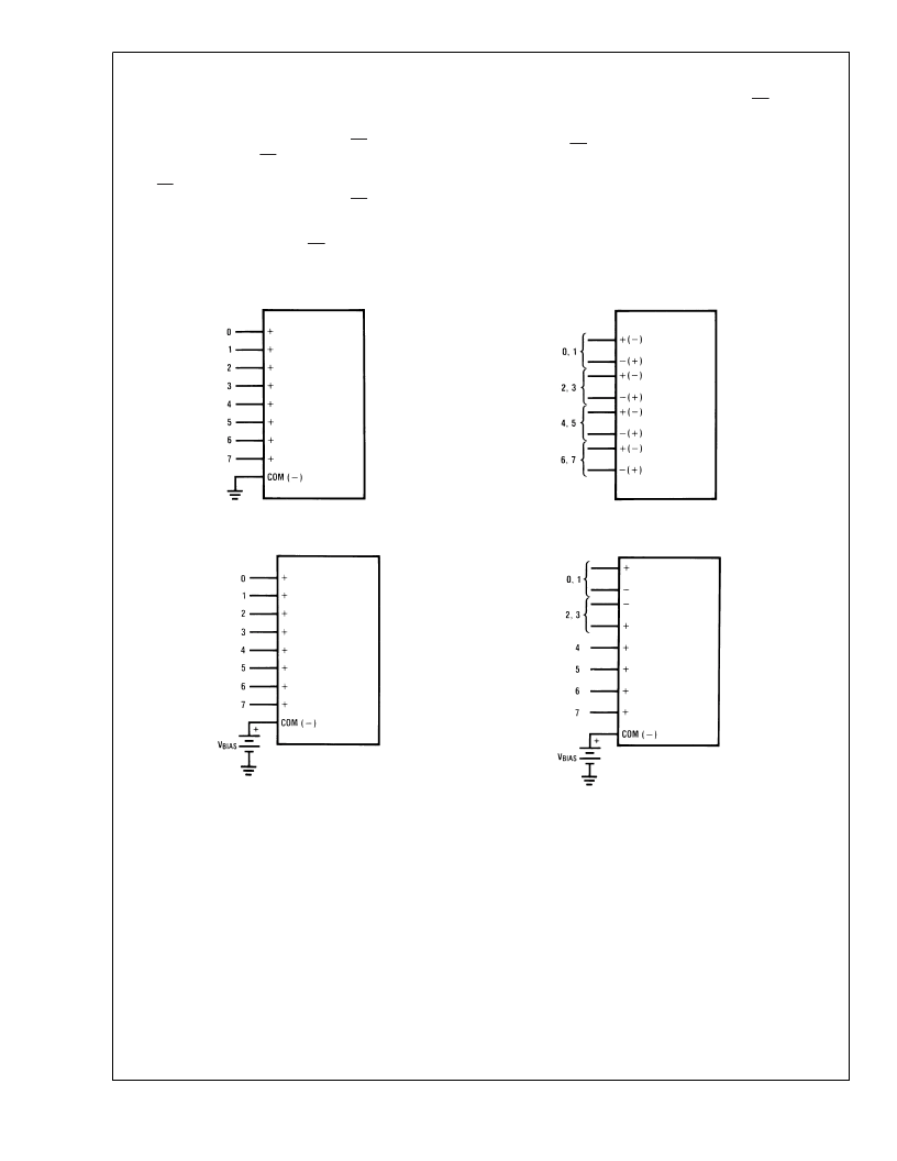
8 Single-Ended
DS010749-41
4 Differential
DS010749-43
8 Psuedo-Differential
DS010749-42
Mixed Mode
DS010749-44
FIGURE 1. Analog Input Multiplexer Options for the ADC08138
A
www.national.com
14
相关PDF资料 |
PDF描述 |
|---|---|
| ADC081500 | High Performance, Low Power, 8-Bit, 1.5 GSPS A/D Converter |
| ADC081500CIYB | High Performance, Low Power, 8-Bit, 1.5 GSPS A/D Converter |
| ADC081500EVAL | High Performance, Low Power, 8-Bit, 1.5 GSPS A/D Converter |
| ADC08161 | 500 ns A/D Converter with S/H Function and 2.5V Bandgap Reference(500ns带S/H功能和2.5V带隙参考的A/D转换器) |
| ADC08161CIWM | 500 ns A/D Converter with S/H Function and 2.5V Bandgap Reference |
相关代理商/技术参数 |
参数描述 |
|---|---|
| ADC08138BIJ | 制造商:未知厂家 制造商全称:未知厂家 功能描述:Single-Ended Data Acquisition System |
| ADC08138BIWM | 制造商:Texas Instruments 功能描述:08138 |
| ADC08138C1WM | 制造商: 功能描述: 制造商:undefined 功能描述: |
| ADC08138CIJ | 制造商:未知厂家 制造商全称:未知厂家 功能描述:Single-Ended Data Acquisition System |
| ADC08138CIWM | 功能描述:IC ADC 8BIT HS SERIAL I/O 20SOIC RoHS:否 类别:集成电路 (IC) >> 数据采集 - 模数转换器 系列:- 产品培训模块:Lead (SnPb) Finish for COTS Obsolescence Mitigation Program 标准包装:2,500 系列:- 位数:12 采样率(每秒):3M 数据接口:- 转换器数目:- 功率耗散(最大):- 电压电源:- 工作温度:- 安装类型:表面贴装 封装/外壳:SOT-23-6 供应商设备封装:SOT-23-6 包装:带卷 (TR) 输入数目和类型:- |
发布紧急采购,3分钟左右您将得到回复。