- 您现在的位置:买卖IC网 > PDF目录298814 > ADC0831CIWM (NATIONAL SEMICONDUCTOR CORP) 1-CH 8-BIT SUCCESSIVE APPROXIMATION ADC, SERIAL ACCESS, PDSO14 PDF资料下载
参数资料
| 型号: | ADC0831CIWM |
| 厂商: | NATIONAL SEMICONDUCTOR CORP |
| 元件分类: | ADC |
| 英文描述: | 1-CH 8-BIT SUCCESSIVE APPROXIMATION ADC, SERIAL ACCESS, PDSO14 |
| 封装: | PLASTIC, SOIC-14 |
| 文件页数: | 20/24页 |
| 文件大小: | 509K |
| 代理商: | ADC0831CIWM |
Electrical Characteristics (Continued)
Note 4: When the input voltage VIN at any pin exceeds the power supplies (VIN < (AGND or DGND) or VIN > VCC) the current at that pin should be limited to 5 mA.
The 20 mA maximum package input current rating limits the number of pins that can safely exceed the power supplies with an input current of 5 mA to four pins.
Note 5: The maximum power dissipation must be derated at elevated temperatures and is dictated by TJMAX, θJA and the ambient temperature, TA. The maximum
allowable power dissipation at any temperature is PD = (TJMAX TA)/θJA or the number given in the Absolute Maximum Ratings, whichever is lower. For devices with
suffixes CIN and CIWM TJMAX = 125C. The typical thermal resistances (θJA) of these parts when board mounted follow: ADC08031CIN 120C/W, ADC08031CIWM
140C/W, ADC08034 CIWM 140C/W, ADC08038CIWM suffixes 91C/W.
Note 6: Human body model, 100 pF capacitor discharged through a 1.5 k
resistor.
Note 7: See AN450 “Surface Mounting Methods and Their Effect on Product Reliability” or Linear Data Book section “Surface Mount” for other methods of soldering
surface mount devices.
Note 8: Typicals are at TJ = 25C and represent the most likely parametric norm.
Note 9: Guaranteed to National’s AOQL (Average Outgoing Quality Level).
Note 10: Total unadjusted error includes offset, full-scale, linearity, multiplexer.
Note 11: For VIN() ≥ VIN(+) the digital code will be 0000 0000. Two on-chip diodes are tied to each analog input (see Block Diagram) which will forward-conduct for
analog input voltages one diode drop below ground or one diode drop greater than VCC supply. During testing at low VCC levels (e.g., 4.5V), high level analog inputs
(e.g., 5V) can cause an input diode to conduct, especially at elevated temperatures, which will cause errors for analog inputs near full-scale. The spec allows 50 mV
forward bias of either diode; this means that as long as the analog VIN does not exceed the supply voltage by more than 50 mV, the output code will be correct. Ex-
ceeding this range on an unselected channel will corrupt the reading of a selected channel. Achievement of an absolute 0 VDC to5VDC input voltage range will there-
fore require a minimum supply voltage of 4.950 VDC over temperature variations, initial tolerance and loading.
Note 12: Channel leakage current is measured after a single-ended channel is selected and the clock is turned off. For off channel leakage current the following two
cases are considered: one, with the selected channel tied high (5 VDC) and the remaining seven off channels tied low (0 VDC), total current flow through the off chan-
nels is measured; two, with the selected channel tied low and the off channels tied high, total current flow through the off channels is again measured. The two cases
considered for determining on channel leakage current are the same except total current flow through the selected channel is measured.
Note 13: A40% to 60% duty cycle range insures proper operation at all clock frequencies. In the case that an available clock has a duty cycle outside of these limits
the minimum time the clock is high or low must be at least 450 ns. The maximum time the clock can be high or low is 100 s.
Note 14: Since data, MSB first, is the output of the comparator used in the successive approximation loop, an additional delay is built in (see Block Diagram) to allow
for comparator response time.
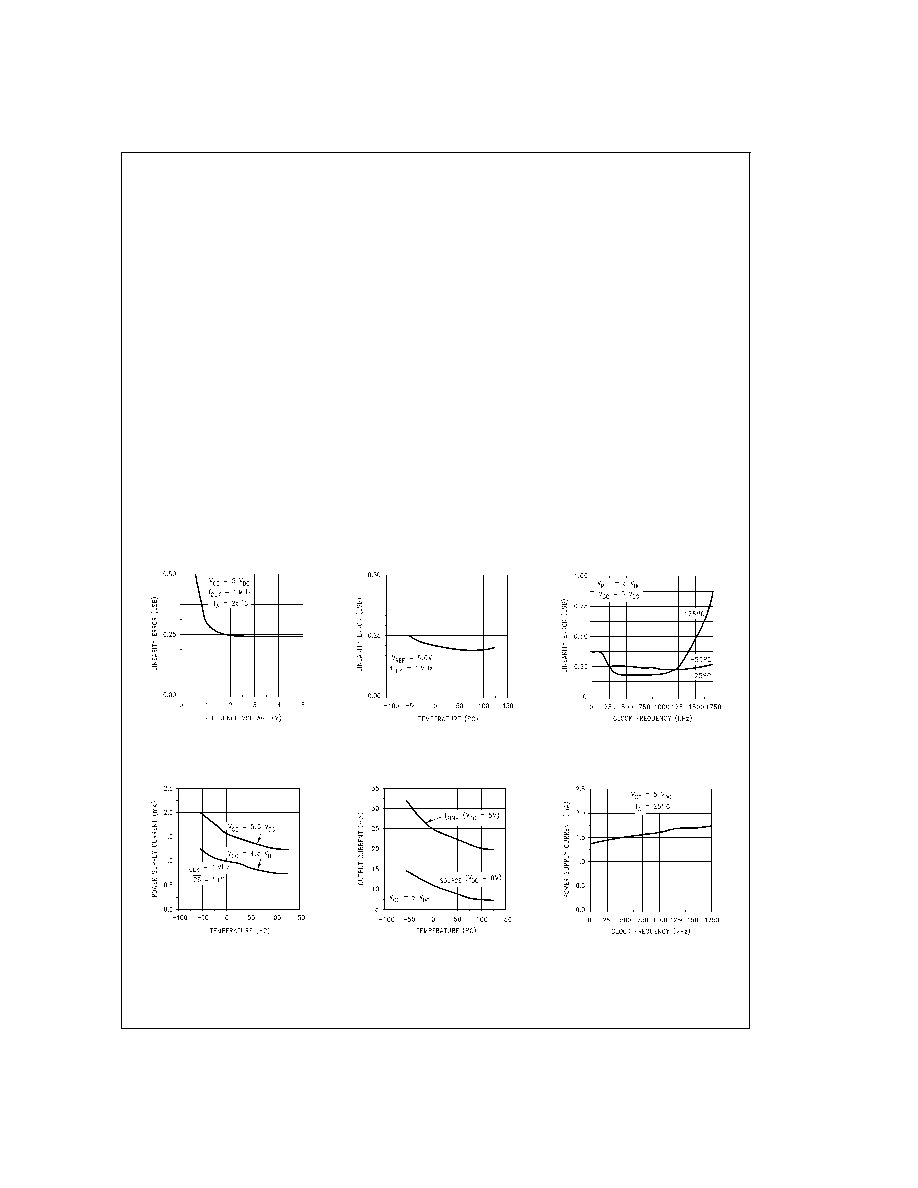
Typical Performance Characteristics
Linearity Error vs
Reference Voltage
DS010555-32
Linearity Error vs
Temperature
DS010555-33
Linearity Error vs
Clock Frequency
DS010555-34
Power Supply Current vs
Temperature
DS010555-35
Output Current vs
Temperature
DS010555-36
Power Supply Current
vs Clock Frequency
DS010555-37
www.national.com
5
相关PDF资料 |
PDF描述 |
|---|---|
| ADE7116ASTZF8-RL | SPECIALTY ANALOG CIRCUIT, PQFP64 |
| ADE7753ARSZRL | SPECIALTY ANALOG CIRCUIT, PDSO20 |
| ADEX-R10+ | 10 MHz - 1000 MHz RF/MICROWAVE DOUBLE BALANCED MIXER, 8.3 dB CONVERSION LOSS-MAX |
| ADF08S | SLIDE DIP SWITCH-8SWITCHES, SPST, LATCHED,SURFACE MOUNT-STRAIGHT |
| ADF09A-KG-TAXB3-R | 9 CONTACT(S), MALE, D SUBMINIATURE CONNECTOR, SOLDER |
相关代理商/技术参数 |
参数描述 |
|---|---|
| ADC0831-N | 制造商:TI 制造商全称:Texas Instruments 功能描述:ADC0831/ADC0832/ADC0834/ADC0838 8-Bit Serial I/O A/D Converters with Multiplexer Options |
| ADC0832 | 制造商:TI 制造商全称:Texas Instruments 功能描述:A/D PERIPHERALS WITH SERIAL CONTROL |
| ADC0832A | 制造商:TI 制造商全称:Texas Instruments 功能描述:A/D PERIPHERALS WITH SERIAL CONTROL |
| ADC0832ACP | 制造商:未知厂家 制造商全称:未知厂家 功能描述:Analog-to-Digital Converter, 8-Bit |
| ADC0832AIP | 制造商:未知厂家 制造商全称:未知厂家 功能描述:Analog-to-Digital Converter, 8-Bit |
发布紧急采购,3分钟左右您将得到回复。