- 您现在的位置:买卖IC网 > PDF目录298814 > ADC0831CIWM (NATIONAL SEMICONDUCTOR CORP) 1-CH 8-BIT SUCCESSIVE APPROXIMATION ADC, SERIAL ACCESS, PDSO14 PDF资料下载
参数资料
| 型号: | ADC0831CIWM |
| 厂商: | NATIONAL SEMICONDUCTOR CORP |
| 元件分类: | ADC |
| 英文描述: | 1-CH 8-BIT SUCCESSIVE APPROXIMATION ADC, SERIAL ACCESS, PDSO14 |
| 封装: | PLASTIC, SOIC-14 |
| 文件页数: | 4/24页 |
| 文件大小: | 509K |
| 代理商: | ADC0831CIWM |
Functional Description (Continued)
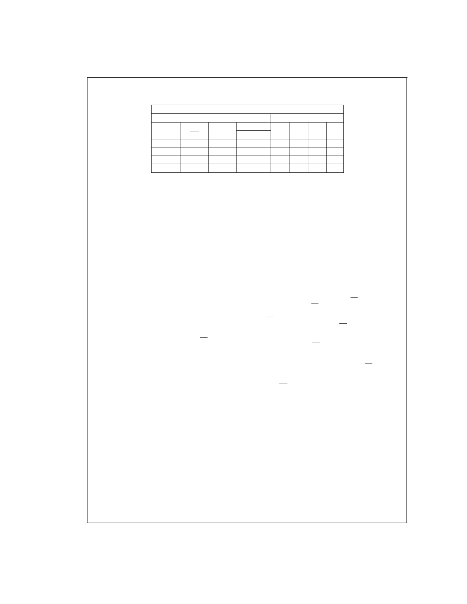
TABLE 4. MUX Addressing: ADC08034
Single-Ended MUX Mode
MUX Address
Channel #
START
SGL/
ODD/
SELECT
0123
DIF
SIGN
1
11
0
+
11
0
1
+
11
1
0
+
11
1
+
COM is internally tied to AGND
Since the input configuration is under software control, it can
be modified as required before each conversion. A channel
can be treated as a single-ended, ground referenced input
for one conversion; then it can be reconfigured as part of a
differential channel for another conversion.
Figure 1 illus-
trates the input flexibility which can be achieved.
The analog input voltages for each channel can range from
50mV below ground to 50mV above V
CC (typically 5V) with-
out degrading conversion accuracy.
2.0 THE DIGITAL INTERFACE
A most important characteristic of these converters is their
serial data link with the controlling processor. Using a serial
communication format offers two very significant system im-
provements; it allows many functions to be included in a
small package and it can eliminate the transmission of low
level analog signals by locating the converter right at the
analog sensor; transmitting highly noise immune digital data
back to the host processor.
To understand the operation of these converters it is best to
refer to the Timing Diagrams and Functional Block Diagram
and to follow a complete conversion sequence. For clarity a
separate timing diagram is shown for each device.
1.
A conversion is initiated by pulling the CS (chip select)
line low. This line must be held low for the entire conver-
sion. The converter is now waiting for a start bit and its
MUX assignment word.
2.
On each rising edge of the clock the status of the data in
(DI) line is clocked into the MUX address shift register.
The start bit is the first logic “1” that appears on this line
(all leading zeros are ignored). Following the start bit the
converter expects the next 2 to 4 bits to be the MUX as-
signment word.
3.
When the start bit has been shifted into the start location
of the MUX register, the input channel has been as-
signed and a conversion is about to begin. An interval of
1
2 clock period (where nothing happens) is automatically
inserted to allow the selected MUX channel to settle.
The SARS line goes high at this time to signal that a con-
version is now in progress and the DI line is disabled (it
no longer accepts data).
4.
The data out (DO) line now comes out of TRI-STATE
and provides a leading zero for this one clock period of
MUX settling time.
5.
During the conversion the output of the SAR comparator
indicates whether the analog input is greater than (high)
or less than (low) a series of successive voltages gener-
ated internally from a ratioed capacitor array (first 5 bits)
and a resistor ladder (last 3 bits). After each comparison
the comparator’s output is shipped to the DO line on the
falling edge of CLK. This data is the result of the conver-
sion being shifted out (with the MSB first) and can be
read by the processor immediately.
6.
After 8 clock periods the conversion is completed. The
SARS line returns low to indicate this 12 clock cycle later.
7.
The stored data in the successive approximation register
is loaded into an internal shift register. If the programmer
prefers the data can be provided in an LSB first format
[this makes use of the shift enable (SE) control line]. On
the ADC08038 the SE line is brought out and if held high
the value of the LSB remains valid on the DO line. When
SE is forced low the data is clocked out LSB first. On de-
vices which do not include the SE control line, the data,
LSB first, is automatically shifted out the DO line after
the MSB first data stream. The DO line then goes low
and stays low until CS is returned high. The ADC08031
is an exception in that its data is only output in MSB first
format.
8.
All internal registers are cleared when the CS line is high
and the t
SELECT requirement is met. See Data Input Tim-
ing under Timing Diagrams. If another conversion is de-
sired CS must make a high to low transition followed by
address information.
The DI and DO lines can be tied together and controlled
through a bidirectional processor I/O bit with one wire.
This is possible because the DI input is only “looked-at”
during the MUX addressing interval while the DO line is
still in a high impedance state.
www.national.com
12
相关PDF资料 |
PDF描述 |
|---|---|
| ADE7116ASTZF8-RL | SPECIALTY ANALOG CIRCUIT, PQFP64 |
| ADE7753ARSZRL | SPECIALTY ANALOG CIRCUIT, PDSO20 |
| ADEX-R10+ | 10 MHz - 1000 MHz RF/MICROWAVE DOUBLE BALANCED MIXER, 8.3 dB CONVERSION LOSS-MAX |
| ADF08S | SLIDE DIP SWITCH-8SWITCHES, SPST, LATCHED,SURFACE MOUNT-STRAIGHT |
| ADF09A-KG-TAXB3-R | 9 CONTACT(S), MALE, D SUBMINIATURE CONNECTOR, SOLDER |
相关代理商/技术参数 |
参数描述 |
|---|---|
| ADC0831-N | 制造商:TI 制造商全称:Texas Instruments 功能描述:ADC0831/ADC0832/ADC0834/ADC0838 8-Bit Serial I/O A/D Converters with Multiplexer Options |
| ADC0832 | 制造商:TI 制造商全称:Texas Instruments 功能描述:A/D PERIPHERALS WITH SERIAL CONTROL |
| ADC0832A | 制造商:TI 制造商全称:Texas Instruments 功能描述:A/D PERIPHERALS WITH SERIAL CONTROL |
| ADC0832ACP | 制造商:未知厂家 制造商全称:未知厂家 功能描述:Analog-to-Digital Converter, 8-Bit |
| ADC0832AIP | 制造商:未知厂家 制造商全称:未知厂家 功能描述:Analog-to-Digital Converter, 8-Bit |
发布紧急采购,3分钟左右您将得到回复。