- 您现在的位置:买卖IC网 > PDF目录378279 > ADC08351 (National Semiconductor Corporation) 8-Bit, 42 MSPS, 40 mW A/D Converter PDF资料下载
参数资料
| 型号: | ADC08351 |
| 厂商: | National Semiconductor Corporation |
| 英文描述: | 8-Bit, 42 MSPS, 40 mW A/D Converter |
| 中文描述: | 8位,42 MSPS的40毫瓦的A / D转换器 |
| 文件页数: | 11/15页 |
| 文件大小: | 492K |
| 代理商: | ADC08351 |
Applications Information
(Continued)
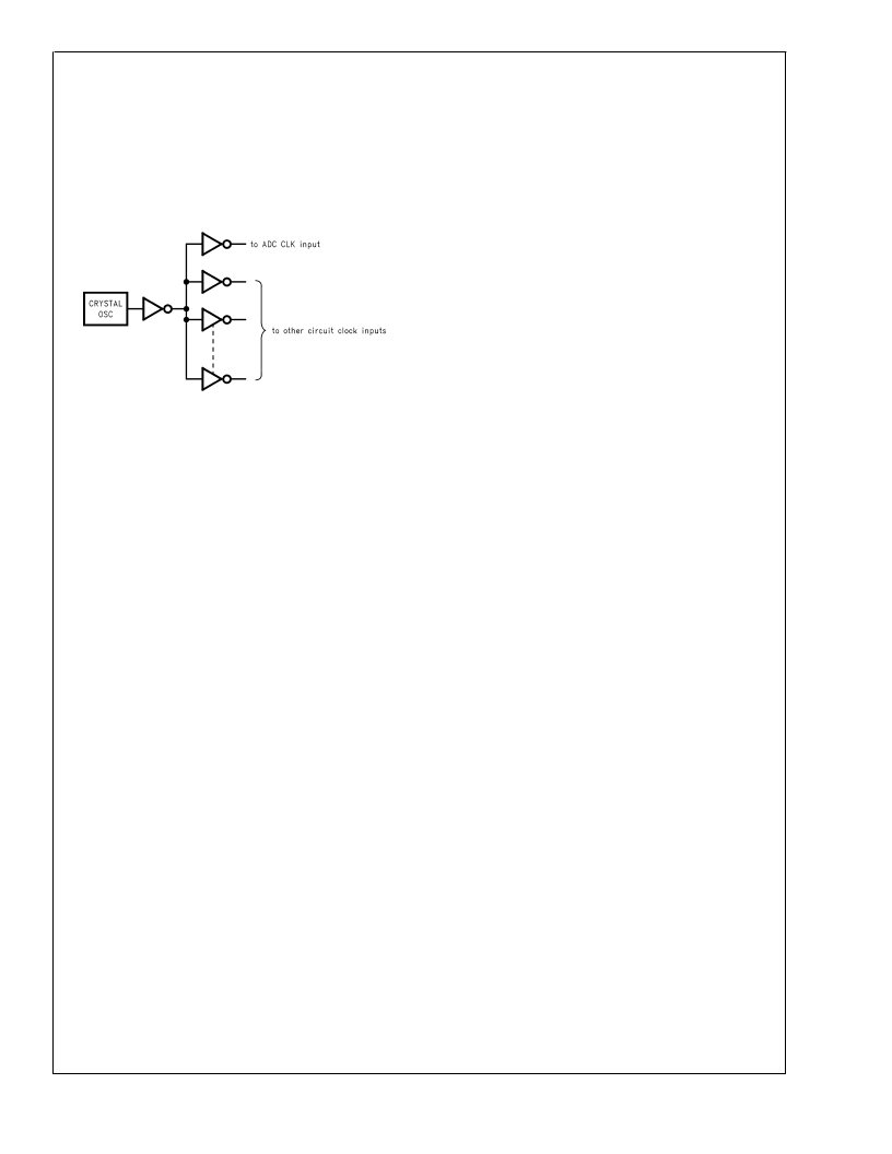
ac performance, isolating the ADC clock from any digital cir-
cuitry should be done with adequate buffers, as with a clock
tree. See Figure 4
It is good practice to keep the ADC clock line as short as
possible and to keep it well away from any other signals.
Other signals can introduce jitter into the clock signal. Even
lines with 90 crossings have capacitive coupling, so try to
avoid even these 90 crossings of the clock line.
Digital circuits create substantial supply and ground current
transients. The logic noise thus generated could have signifi-
cant impact upon system noise performance. The best logic
family to use in systems with A/D converters is one which
employs non-saturating transistor designs, or has low noise
characteristics, such as the 74HC(T) and 74AC(T)Q families.
The worst noise generators are logic families that draw the
largest supply current transients during clock or signal
edges, like the 74F and the 74AC(T) families. In general,
slower logic families, such as 74LS and 74HC(T) will pro-
duce less high frequency noise than do high speed logic
families, such as the 74F and 74AC(T) families.
Since digital switching transients are composed largely of
high frequency components, total ground plane copper
weight will have little effect upon the logic-generated noise.
This is because of the skin effect. Total surface area is more
important than is total ground plane volume.
An effective way to control ground noise is by connecting the
analog and digital ground planes together beneath the ADC
with a copper trace that is narrow compared with the rest of
the ground plane. This narrowing beneath the converter pro-
vides a fairly high impedance to the high frequency compo-
nents of the digital switching currents, directing them away
from the analog pins. The relatively lower frequency analog
ground currents do not create a significant variation across
the impedance of this relatively narrow ground connection.
5.0 TYPICAL APPLICATION CIRCUITS
Figure 5 shows a simple interface for a low impedance
source located close to the converter. As discussed in Sec-
tion 1.0, the series capacitor is optional. Notice the isolation
of the ADC clock signal from the clock signals going else-
where in the system. The reference input of this circuit is
shown connected to the 3V supply.
Video ADCs tend to have input current transients that can
upset a driving source, causing distortion of the driving sig-
nal. The resistor at the ADC08351 input isolates the amplifi-
er’s output from the current transients at the input to the con-
verter.
When the signal source is not located close to the converter,
the signal should be buffered. Figure 6 shows an example of
an appropriate buffer. The amplifier provides a gain of two to
compensate for transmission losses.
Operational amplifiers have better linearity when they oper-
ate with gain, so the input is attenuated with the 68
and
30
resistors at the non-inverting input. The 330
resistor in
parallel with these two resistors provides for a 75
cable ter-
mination. Replacing this 330
resistor with one of 100
will
provide a 50
termination.
The circuit shown has a nominal gain of two. You can provide
a gain adjustment by changing the 110
feedback resistor to
a 100
resistor in series with a 20
potentiometer.
The offset adjustment is used to bring the input signal within
the common mode range of the converter. If a fixed offset is
desired, the potentiometer and the 3.3k resistor may be re-
placed with a single resistor of 3k to 4k to the appropriate
supply. The resistor value and the supply polarity used will
depend upon the amount and polarity of offset needed.
The CLC409 shown in Figure 6 was chosen for a low cost
solution with good overall performance.
Figure 7 shows an inverting DC coupled circuit. The above
comments regarding Figure 6 generally apply to this circuit
as well.
DS100895-26
FIGURE 4. Isolating the ADC Clock from Digital
Circuitry
A
www.national.com
11
相关PDF资料 |
PDF描述 |
|---|---|
| ADC08351CIMTC | 8-Bit, 42 MSPS, 40 mW A/D Converter |
| ADC08351CIMTCX | 8-Bit, 42 MSPS, 40 mW A/D Converter |
| ADC0841 | 8-Bit P Compatible A/D Converter |
| ADC0841BCN | 8-Bit P Compatible A/D Converter |
| ADC0841BCV | 8-Bit P Compatible A/D Converter |
相关代理商/技术参数 |
参数描述 |
|---|---|
| ADC08351_03 | 制造商:NSC 制造商全称:National Semiconductor 功能描述:8-Bit, 42 MSPS, 40 mW A/D Converter |
| ADC08351CILQ | 制造商:NSC 制造商全称:National Semiconductor 功能描述:8-Bit, 42 MSPS, 40 mW A/D Converter |
| ADC08351CILQ/NOPB | 功能描述:IC ADC 8BIT 42MSPS 24-LLP RoHS:是 类别:集成电路 (IC) >> 数据采集 - 模数转换器 系列:- 产品培训模块:Lead (SnPb) Finish for COTS Obsolescence Mitigation Program 标准包装:2,500 系列:- 位数:12 采样率(每秒):3M 数据接口:- 转换器数目:- 功率耗散(最大):- 电压电源:- 工作温度:- 安装类型:表面贴装 封装/外壳:SOT-23-6 供应商设备封装:SOT-23-6 包装:带卷 (TR) 输入数目和类型:- |
| ADC08351CILQX | 功能描述:模数转换器 - ADC RoHS:否 制造商:Texas Instruments 通道数量:2 结构:Sigma-Delta 转换速率:125 SPs to 8 KSPs 分辨率:24 bit 输入类型:Differential 信噪比:107 dB 接口类型:SPI 工作电源电压:1.7 V to 3.6 V, 2.7 V to 5.25 V 最大工作温度:+ 85 C 安装风格:SMD/SMT 封装 / 箱体:VQFN-32 |
| ADC08351CILQX/NOPB | 功能描述:模数转换器 - ADC RoHS:否 制造商:Texas Instruments 通道数量:2 结构:Sigma-Delta 转换速率:125 SPs to 8 KSPs 分辨率:24 bit 输入类型:Differential 信噪比:107 dB 接口类型:SPI 工作电源电压:1.7 V to 3.6 V, 2.7 V to 5.25 V 最大工作温度:+ 85 C 安装风格:SMD/SMT 封装 / 箱体:VQFN-32 |
发布紧急采购,3分钟左右您将得到回复。