- 您现在的位置:买卖IC网 > PDF目录378279 > ADC0851BIN (NATIONAL SEMICONDUCTOR CORP) 8-Bit Analog Data Acquisition and Monitoring Systems PDF资料下载
参数资料
| 型号: | ADC0851BIN |
| 厂商: | NATIONAL SEMICONDUCTOR CORP |
| 元件分类: | ADC |
| 英文描述: | 8-Bit Analog Data Acquisition and Monitoring Systems |
| 中文描述: | 2-CH 8-BIT SUCCESSIVE APPROXIMATION ADC, SERIAL ACCESS, PDIP16 |
| 封装: | PLASTIC, DIP-16 |
| 文件页数: | 15/36页 |
| 文件大小: | 581K |
| 代理商: | ADC0851BIN |
第1页第2页第3页第4页第5页第6页第7页第8页第9页第10页第11页第12页第13页第14页当前第15页第16页第17页第18页第19页第20页第21页第22页第23页第24页第25页第26页第27页第28页第29页第30页第31页第32页第33页第34页第35页第36页
1.0 Modes of Operation
(Continued)
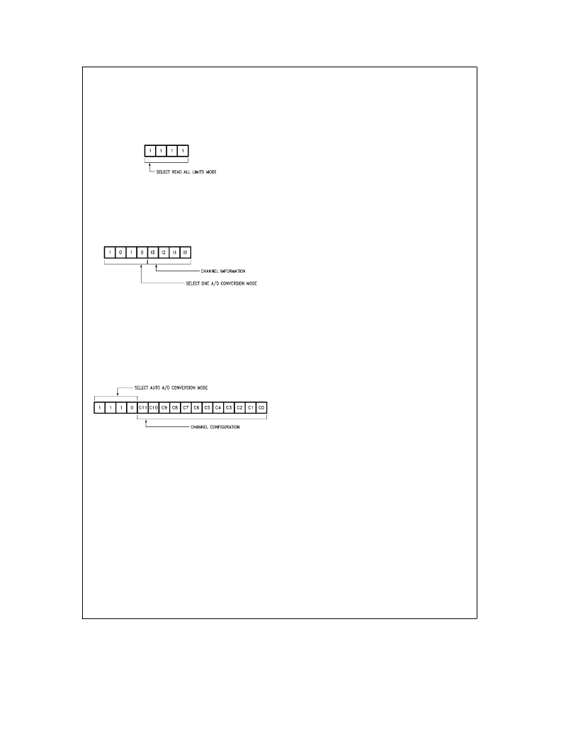
1.5 READ ALL LIMITS FROM RAM
This mode of operation allows the device to serially output
8-bit limit data from each memory location in succession
starting with CH0-lower limit (see Section 2.4 under inter-
face considerations).
Data Input (DI) WordDADC0851 or ADC0858
TL/H/11021–27
1.6 INITIATE ONE A/D CONVERSION
At any time, the user can initiate an A/D conversion on any
input channel. Note that the input channels may be config-
ured as single ended or differential inputs. The first four bits
of the input word select the mode of operation and the next
four bits assign the multiplexer configuration.
Data Input (DI) WordDADC0851 or ADC0858
TL/H/11021–28
1.7 INITIATE AUTO A/D CONVERSION
When configured in this mode, an A/D conversion is done
on a channel or channel pair and after the output data is
transmitted, conversion begins on the next subsequent
channel or channel pair. In this mode the device continually
scans through the input channels making A/D conversions
unless the device’s mode of operation is changed. The first
four bits of the input word select the mode of operation and
the next twelve bits assign the multiplexer configuration.
Data Input (DI) WordDADC0851 or ADC0858
TL/H/11021–29
1.8 TEST MODE
This mode is used to test the ADC0851/8 at the factory and
is
not
intended for normal use. If this mode is accidentally
selected, the supply voltage must be disconnected and then
reconnected to reset the device.
2.0 Conversion Timing vs
Serial Interface Timing
Note that the ADC0851/8 uses two clock signals for proper
operation. Connecting an external resister (R
ext
) from the
OSC pin (pin 2) to V
CC
and an external capacitor (C
ext
) from
the OSC pin to ground causes the device’s internal oscilla-
tor to generate the OSC clock signal for A/D conversion
and watchdog timing. With R
ext
e
3.16 k
X
and C
ext
e
170 pF, the OSC clock frequency is approximately 1 MHz.
Note that internally, ADC0851/8 divides the OSC clock fre-
quency by two. An A/D conversion is completed in eighteen
OSC clock periods maximum. It should be noted that the
OSC pin of the ADC0851/8 should not be driven by an ex-
ternal clock.
An external clock signal is applied to the CLK pin (pin 4) of
the ADC0851/8. The CLK signal is used to clock serial data
either into the data input pin (DI) or out of the data output
pin (DO).
Note that input data is loaded at the rising edge of CLK
while the output data is valid at the falling edge of CLK. All
digital timing such as data set-up and hold times and delays
are measured with respect to the CLK signal. The OSC
clock and CLK frequencies need not be the same.
3.0 Programming Information
The ADC0851 and ADC0858 communicate data serially
over the DI (data input) and DO (data output) lines. The data
format for the input and output words for various modes of
operation are shown in the ‘‘programming charts.’’
There are nine types of data as shown in the ‘‘serial com-
munication bit order’’ table. The order in which data is com-
municated is MSB first in all but two cases: Limit data and
A/D conversion data. The various data types are described
below.
3.1 LIMIT DATA (L0, L1, . . . L7)
Limits on the ADC0851/8 are 8 bits in width and can either
represent an upper or lower boundary limit. Limit data can
either be written (in the ‘‘write one limit’’ or ‘‘write all limits’’
mode) to or read (in the ‘‘read one limit’’ or ‘‘read all limits’’
mode) from the limit RAM. Being able to read back the limit
data allows system testability, and it also allows indepen-
dent software routines to see what window limits were previ-
ously written to the chip. During watchdog operation, a pro-
grammed limit must be crossed in order to cause an inter-
rupt.
3.2 A/D CONVERSION DATA (D0, D1, . . . D7)
There are two A/D conversion modes (One A/D conversion
and Auto A/D conversion) that produce 8-bit conversion
data. During either type of A/D conversion, a single-ended
analog input or a differential analog input pair is digitized to
produce this conversion data.
3.3 LIMIT ADDRESS (A3, A2, . . . A0)
The limit address points to the location, within the limit
RAM, to which limit data is sent or from which it is received.
Limit address is used in the ‘‘write one limit to RAM’’, ‘‘write
all limits to RAM’’, ‘‘read one limit from RAM’’ or ‘‘read all
limits from RAM’’ mode. There are two addresses for each
analog input; the even addresses correspond to the lower
15
相关PDF资料 |
PDF描述 |
|---|---|
| ADC0851BIV | 8-Bit Analog Data Acquisition and Monitoring Systems |
| ADC0851CIN | 8-Bit Analog Data Acquisition and Monitoring Systems |
| ADC0851CIV | 8-Bit Analog Data Acquisition and Monitoring Systems |
| ADC0858CIN | 8-Bit Analog Data Acquisition and Monitoring Systems |
| ADC0858CIV | 8-Bit Analog Data Acquisition and Monitoring Systems |
相关代理商/技术参数 |
参数描述 |
|---|---|
| ADC0851BIV | 制造商:NSC 制造商全称:National Semiconductor 功能描述:8-Bit Analog Data Acquisition and Monitoring Systems |
| ADC0851CIJ | 制造商:未知厂家 制造商全称:未知厂家 功能描述:Single-Ended Data Acquisition System |
| ADC0851CIN | 制造商:NSC 制造商全称:National Semiconductor 功能描述:8-Bit Analog Data Acquisition and Monitoring Systems |
| ADC0851CIV | 制造商:NSC 制造商全称:National Semiconductor 功能描述:8-Bit Analog Data Acquisition and Monitoring Systems |
| ADC0851CMJ/883 | 制造商:未知厂家 制造商全称:未知厂家 功能描述:Single-Ended Data Acquisition System |
发布紧急采购,3分钟左右您将得到回复。