- 您现在的位置:买卖IC网 > PDF目录378279 > ADC0851BIV (NATIONAL SEMICONDUCTOR CORP) 8-Bit Analog Data Acquisition and Monitoring Systems PDF资料下载
参数资料
| 型号: | ADC0851BIV |
| 厂商: | NATIONAL SEMICONDUCTOR CORP |
| 元件分类: | ADC |
| 英文描述: | 8-Bit Analog Data Acquisition and Monitoring Systems |
| 中文描述: | 2-CH 8-BIT SUCCESSIVE APPROXIMATION ADC, SERIAL ACCESS, PQCC20 |
| 封装: | PLASTIC, LCC-20 |
| 文件页数: | 18/36页 |
| 文件大小: | 581K |
| 代理商: | ADC0851BIV |
第1页第2页第3页第4页第5页第6页第7页第8页第9页第10页第11页第12页第13页第14页第15页第16页第17页当前第18页第19页第20页第21页第22页第23页第24页第25页第26页第27页第28页第29页第30页第31页第32页第33页第34页第35页第36页
2.0 Memory Access Modes
The ADC0851/8 has an internal RAM with sixteen memory
locations (one location for the upper limit and one for the
lower limit for each of the 8 input channels). Each memory
location is 8 bits wide. An 8-bit limit word representing an
upper or lower limit boundary can either be written to or read
from the RAM. The ADC0851 uses only four memory loca-
tions for the four boundary limits corresponding to the two
inputs. The eight channel ADC0858, however, makes use of
all sixteen memory locations.
Each memory location is accessed by a specific address as
shown by Table II(a) and (b). Note that even addresses cor-
respond to the lower limits while the odd addresses corre-
spond to the upper limits. The ADC0851 and ADC0858 both
use 4 bits (A3, . . . A0) to address the RAM, however,
ADC0851 decodes only the two LSBs of the address data
while ignoring the two MSBs.
TABLE IIa. RAM Address and
Limit Data for ADC0851
RAM Address
Corresponding
Channel and Limit
A3
A2
A1
A0
X
X
0
0
CH0–Lower Limit
X
X
0
1
CH0–Upper Limit
X
X
1
0
CH1–Lower Limit
X
X
1
1
CH1–Upper Limit
Limit Data (ADC0851)
L0
L1
L2
L3
L4
L5
L6
L7
TABLE IIb. RAM Address and
Limit Data for ADC0858
RAM Address
Corresponding
Channel and Limit
A3
A2
A1
A0
0
0
0
0
CH0–Lower Limit
0
0
0
1
CH0–Upper Limit
0
0
1
0
CH1–Lower Limit
0
0
1
1
CH1–Upper Limit
0
1
0
0
CH2–Lower Limit
0
1
0
1
CH2–Upper Limit
0
1
1
0
CH3–Lower Limit
0
1
1
1
CH3–Upper Limit
1
0
0
0
CH4–Lower Limit
1
0
0
1
CH4–Upper Limit
1
0
1
0
CH5–Lower Limit
1
0
1
1
CH5–Upper Limit
1
1
0
0
CH6–Lower Limit
1
1
0
1
CH6–Upper Limit
1
1
1
0
CH7–Lower Limit
1
1
1
1
CH7–Upper Limit
Limit Data (ADC0858)
L0
L1
L2
L3
L4
L5
L6
L7
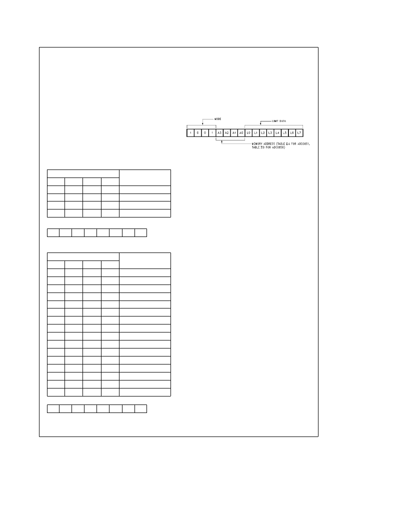
2.1 WRITE ONE LIMIT
This mode is used to update a single memory location in the
limit RAM. An 8-bit limit word is written to the location point-
ed to by the limit address. From Table I we can see that to
initiate the operation of the device in the ‘‘write one limit’’
mode, the mode address has to be 1 0 0 1. The data format
for the input word is as shown below.
Data Input (DI) WordDADC0851 or ADC0858
TL/H/11021–31
18
相关PDF资料 |
PDF描述 |
|---|---|
| ADC0851CIN | 8-Bit Analog Data Acquisition and Monitoring Systems |
| ADC0851CIV | 8-Bit Analog Data Acquisition and Monitoring Systems |
| ADC0858CIN | 8-Bit Analog Data Acquisition and Monitoring Systems |
| ADC0858CIV | 8-Bit Analog Data Acquisition and Monitoring Systems |
| ADC0881 | 8-Bit 20 MSPS Flash A/D Converter |
相关代理商/技术参数 |
参数描述 |
|---|---|
| ADC0851CIJ | 制造商:未知厂家 制造商全称:未知厂家 功能描述:Single-Ended Data Acquisition System |
| ADC0851CIN | 制造商:NSC 制造商全称:National Semiconductor 功能描述:8-Bit Analog Data Acquisition and Monitoring Systems |
| ADC0851CIV | 制造商:NSC 制造商全称:National Semiconductor 功能描述:8-Bit Analog Data Acquisition and Monitoring Systems |
| ADC0851CMJ/883 | 制造商:未知厂家 制造商全称:未知厂家 功能描述:Single-Ended Data Acquisition System |
| ADC0852 | 制造商:NSC 制造商全称:National Semiconductor 功能描述:Multiplexed Comparator with 8-Bit Reference Divider |
发布紧急采购,3分钟左右您将得到回复。