- 您现在的位置:买卖IC网 > PDF目录378279 > ADC0852 (NATIONAL SEMICONDUCTOR CORP) Synchronous 4-Bit Up/Down Counters With Up/Down Mode Control 16-PDIP 0 to 70 PDF资料下载
参数资料
| 型号: | ADC0852 |
| 厂商: | NATIONAL SEMICONDUCTOR CORP |
| 元件分类: | 模拟信号调理 |
| 英文描述: | Synchronous 4-Bit Up/Down Counters With Up/Down Mode Control 16-PDIP 0 to 70 |
| 中文描述: | SPECIALTY ANALOG CIRCUIT, PDIP8 |
| 封装: | DIP-8 |
| 文件页数: | 13/20页 |
| 文件大小: | 327K |
| 代理商: | ADC0852 |
Functional Description
(Continued)
4.0 ANALOG INPUTS
4. 1 Differential Inputs
The serial interface of the ADC0852 and ADC0854 allows
them to be located right at the analog signal source and to
communicate with a controlling processor via a few fairly
noise immune digital lines. This feature in itself greatly re-
duces the analog front end circuitry often needed to main-
tain signal integrity. Nevertheless, a few words are in order
with regard to the analog inputs should the input be noisy to
begin with or possibly riding on a large common mode volt-
age.
The differential input of the comparator actually reduces the
effect of common-mode input noise, i.e. signals common to
both selected ‘‘
a
’’ and ‘‘
b
’’ inputs such as 60 Hz line
noise. The time interval between sampling the ‘‘
a
’’ input
and then the ‘‘
b
’’ input is
(/2
of a clock period (see Figure
5).
The change in the common-mode voltage during this short
time interval can cause comparator errors. For a sinusoidal
common-mode signal this error is:
V
ERROR
(MAX)
e
V
PEAK
(2
q
f
CM
/2 f
CLK
)
where f
CM
is the frequency of the common-mode signal,
V
peak
is its peak voltage value, and f
CLK
is the DAC clock
frequency.
For example, 1 V
PP
60 Hz noise superimposed on both
sides of a differential input signal would cause an error (re-
ferred to the input) of 0.75 mV. This amounts to less than
(/25
of an LSB referred to the threshold DAC, (assuming
V
REF
e
5V and f
CLK
e
250 kHz).
4. 2 Input Currents and Filtering
Due to the sampling nature of the analog inputs, short
spikes of current enter the ‘‘
a
’’ input and leave the ‘‘
b
’’ at
the clock edges during a comparison. These currents decay
rapidly and do not cause errors as the comparator is
strobed at the end of the clock period (see Figure 5).
The source resistance of the analog input is important with
regard to the DC leakage currents of the input multiplexer.
The worst-case leakage currents of
g
1
m
A over tempera-
ture will create a 1 mV input error with a 1 k
X
source
resistance. An op-amp RC active low pass filter can provide
both impedance buffering and noise filtering should a high
impedance source be required.
4. 3 Arbitrary Analog Input/Reference Range
The total span of the DAC output and hence the compara-
tor’s threshold voltage is determined by the DAC reference.
For example, if V
REF
is set to 1 volt then the comparator’s
threshold can be programmed over a 0 to 1 volt range with
8 bits of resolution. From the analog input’s point of view,
this span can also be shifted by applying an offset potential
to one of the comparator’s selected analog input lines (usu-
ally ‘‘
b
’’). This gives the designer greater control of the
ADC0852/4’s input range and resolution and can help sim-
plify or eliminate expensive signal conditioning electronics.
An example of this capability is shown in the ‘‘Load Cell
Limit Comparator’’ ofFigure 15. In this circuit, the ADC0852
allows the load-cell signal conditioning to be done with only
one dual op-amp and without complex, multiple resistor
matching.
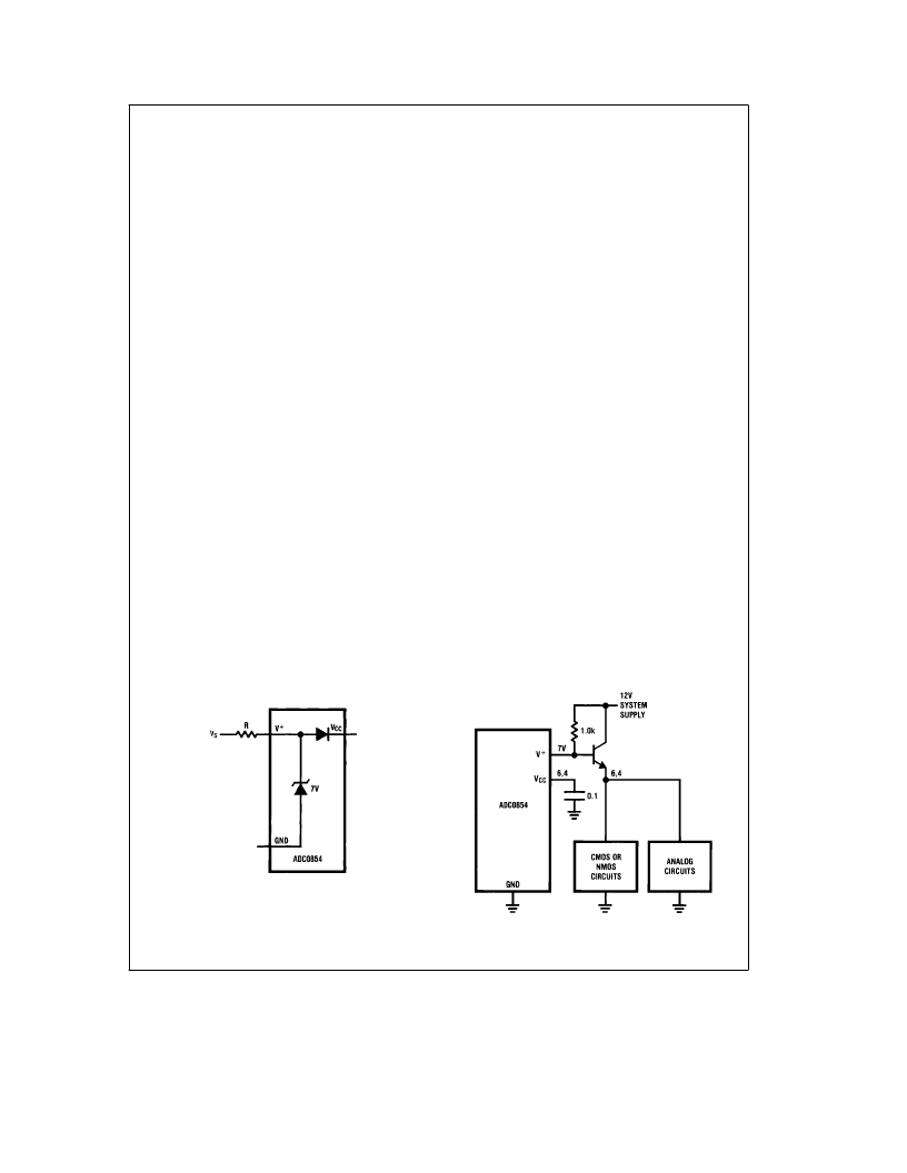
5.0 POWER SUPPLY
A unique feature of the ADC0854 is the inclusion of a 7 volt
zener diode connected from the ‘‘V
a
’’ terminal to ground
(Figures 2 and8) ‘‘V
a
’’ also connects to ‘‘V
CC
’’ via a silicon
diode. The zener is intended for use as a shunt voltage
regulator to eliminate the need for additional regulating
components. This is especially useful if the ADC0854 is to
be remotely located from the system power source.
An important use of the interconnecting diode between V
a
and V
CC
is shown in Figures 10 and 11. Here this diode is
used as a rectifier to allow the V
CC
supply for the converter
to be derived from the comparator clock. The low device
current requirements and the relatively high clock frequen-
cies used (10 kHz–400 kHz) allows use of the small value
filter capacitor shown. The shunt zener regulator can also
be used in this mode however this requires a clock voltage
swing in excess of 7 volts. Current limiting for the zener is
also needed, either built into the clock generator or through
a resistor connected from the clock to V
a
.
Typical Applications
TL/H/5521–17
FIGURE 8. An On-Chip Shunt Regulator Diode
TL/H/5521–18
FIGURE 9. Using the ADC0854 as the
System Supply Regulator
13
相关PDF资料 |
PDF描述 |
|---|---|
| ADC0852CCN | Multiplexed Comparator with 8-Bit Reference Divider |
| ADC0858BIN | 8-Bit Analog Data Acquisition and Monitoring Systems |
| ADC0858BIV | 8-Bit Analog Data Acquisition and Monitoring Systems |
| ADC0851 | 8-Bit Analog Data Acquisition and Monitoring Systems |
| ADC0851BIN | 8-Bit Analog Data Acquisition and Monitoring Systems |
相关代理商/技术参数 |
参数描述 |
|---|---|
| ADC0852BCJ/A+ | 制造商:未知厂家 制造商全称:未知厂家 功能描述:Analog Comparator |
| ADC0852BCN | 制造商:未知厂家 制造商全称:未知厂家 功能描述:Analog Comparator |
| ADC0852BCN/A+ | 制造商:未知厂家 制造商全称:未知厂家 功能描述:Analog Comparator |
| ADC0852BCN/B+ | 制造商:未知厂家 制造商全称:未知厂家 功能描述:Analog Comparator |
| ADC0852BJ | 制造商:未知厂家 制造商全称:未知厂家 功能描述:Analog Comparator |
发布紧急采购,3分钟左右您将得到回复。