- 您现在的位置:买卖IC网 > PDF目录378279 > ADC0852 (NATIONAL SEMICONDUCTOR CORP) Synchronous 4-Bit Up/Down Counters With Up/Down Mode Control 16-PDIP 0 to 70 PDF资料下载
参数资料
| 型号: | ADC0852 |
| 厂商: | NATIONAL SEMICONDUCTOR CORP |
| 元件分类: | 模拟信号调理 |
| 英文描述: | Synchronous 4-Bit Up/Down Counters With Up/Down Mode Control 16-PDIP 0 to 70 |
| 中文描述: | SPECIALTY ANALOG CIRCUIT, PDIP8 |
| 封装: | DIP-8 |
| 文件页数: | 4/20页 |
| 文件大小: | 327K |
| 代理商: | ADC0852 |
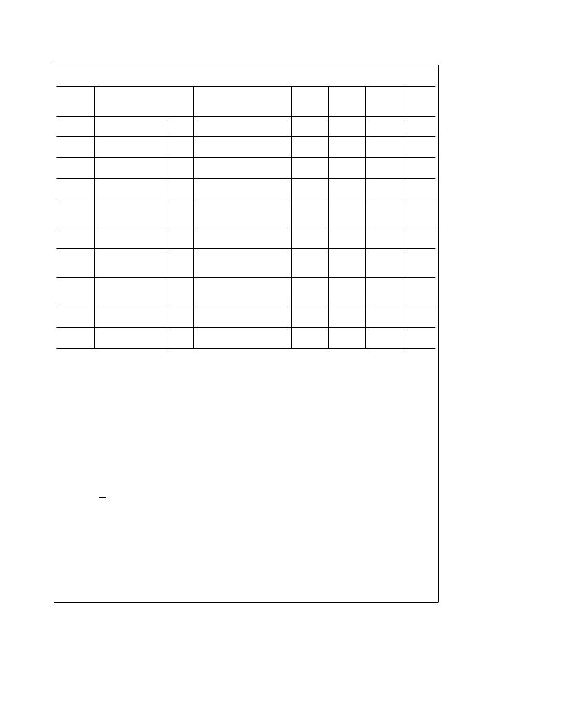
AC Characteristics
t
r
e
t
f
e
20 ns, T
A
e
25
§
C
Typ
Tested
Limit
(Note 5)
Design
Limit
(Note 6)
Symbol
Parameter
Conditions
(Note 4)
Units
f
CLK
Clock Frequency
(Note 12)
MIN
MAX
10
kHz
kHz
400
t
D1
Rising Edge of Clock
to ‘‘DO’’ Enabled
C
L
e
100 pF
650
1000
ns
t
r
Comparator Response
Time (Note 13)
Not Including
Addressing Time
2
a
1
m
s
1/f
CLK
Clock Duty Cycle
(Note 10)
MIN
MAX
40
60
%
%
t
SET-UP
CS Falling Edge or
Data Input Valid to
CLK Rising Edge
MAX
250
ns
t
HOLD
Data Input Valid after
CLK Rising Edge
MIN
90
ns
t
pd1
, t
pd0
CLK Falling Edge to
Output Data Valid
(Note 11)
MAX
C
L
e
100 pF
650
1000
ns
t
1H
, t
0H
Rising Edge of CS to
Data Output Hi-Z
MAX
C
L
e
10 pF, R
L
e
10k
C
L
e
100 pF, R
L
e
2k
(see TRI-STATE Test Circuits)
125
250
500
ns
ns
500
C
IN
Capacitance of Logic
Input
5
pF
C
OUT
Capacitance of Logic
Outputs
5
pF
Note 1:
Absolute Maximum Ratings indicate limits beyond which damage to the device may occur. DC and AC electrical specifications do not apply when
operating the device beyond its specified operating conditions.
Note 2:
All voltages are measured with respect to ground.
Note 3:
Internal zener diodes (approx. 7V) are connected from V
a
to GND and V
CC
to GND. The zener at V
a
can operate as a shunt regulator and is connected
to V
CC
via a conventional diode. Since the zener voltage equals the A/D’s breakdown voltage, the diode ensures that V
CC
will be below breakdown when the
device is powered from V
a
. Functionality is therefore guaranteed for V
a
operation even though the resultant voltage at V
CC
may exceed the specified Absolute
Max of 6.5V. It is recommended that a resistor be used to limit the max current into V
a
.
Note 4:
Typicals are at 25
§
C and represent most likely parametric norm.
Note 5:
Tested and guaranteed to National AOQL (Average Outgoing Quality Level).
Note 6:
Guaranteed, but not 100% production tested. These limits are not used to calculate outgoing quality levels.
Note 7:
Total unadjusted error includes comparator offset, DAC linearity, and multiplexer error. It is expressed in LSBs of the threshold DAC’s input code.
Note 8:
For V
IN
(
b
)
t
V
IN
(
a
) the output will be 0. Two on-chip diodes are tied to each analog input (see Block Diagram) which will forward conduct for analog input
voltages one diode drop below ground or one diode drop greater than the V
CC
supply. Be careful, during testing at low V
CC
levels (4.5V), as high level analog inputs
(5V) can cause this input diode to conductDespecially at elevated temperatures, and cause errors for analog inputs near full-scale. The spec allows 50 mV forward
bias of either diode. This means that as long as the analog V
IN
or V
REF
does not exceed the supply voltage by more than 50 mV, the output code will be correct. To
achieve an absolute 0 V
DC
to 5 V
DC
input voltage range will therefore require a minimum supply voltage of 4.950 V
DC
over temperature variations, initial tolerance
and loading.
Note 9:
Leakage current is measured with the clock not switching.
Note 10:
A 40% to 60% clock duty cycle range ensures proper operation at all clock frequencies. In the case that an available clock has a duty cycle outside of
these limits then 1.6
m
S
s
CLK Low
s
60
m
S and 1.6
m
S
s
CLK HIGH
s
%
.
Note 11:
With CS low and programming complete, D0 is updated on each falling CLK edge. However, each new output is based on the comparison completed 0.5
clock cycles prior (see Figure 5).
Note 12:
Error specs are not guaranteed at 400 kHz (see graph: Comparator Error vs. f
CLK
).
Note 13:
See text, section 1.2.
Note 14:
Human body model, 100 pF discharged through a 1.5 k
X
resistor.
Note 15:
Because the reference ladder of the ADC0852 is internally connected to V
CC
, ladder resistance cannot be directly tested for the ADC0852. Ladder
current is included in the ADC0852’s supply current specification.
4
相关PDF资料 |
PDF描述 |
|---|---|
| ADC0852CCN | Multiplexed Comparator with 8-Bit Reference Divider |
| ADC0858BIN | 8-Bit Analog Data Acquisition and Monitoring Systems |
| ADC0858BIV | 8-Bit Analog Data Acquisition and Monitoring Systems |
| ADC0851 | 8-Bit Analog Data Acquisition and Monitoring Systems |
| ADC0851BIN | 8-Bit Analog Data Acquisition and Monitoring Systems |
相关代理商/技术参数 |
参数描述 |
|---|---|
| ADC0852BCJ/A+ | 制造商:未知厂家 制造商全称:未知厂家 功能描述:Analog Comparator |
| ADC0852BCN | 制造商:未知厂家 制造商全称:未知厂家 功能描述:Analog Comparator |
| ADC0852BCN/A+ | 制造商:未知厂家 制造商全称:未知厂家 功能描述:Analog Comparator |
| ADC0852BCN/B+ | 制造商:未知厂家 制造商全称:未知厂家 功能描述:Analog Comparator |
| ADC0852BJ | 制造商:未知厂家 制造商全称:未知厂家 功能描述:Analog Comparator |
发布紧急采购,3分钟左右您将得到回复。