- 您现在的位置:买卖IC网 > PDF目录378279 > ADC0858CIN (NATIONAL SEMICONDUCTOR CORP) 8-Bit Analog Data Acquisition and Monitoring Systems PDF资料下载
参数资料
| 型号: | ADC0858CIN |
| 厂商: | NATIONAL SEMICONDUCTOR CORP |
| 元件分类: | ADC |
| 英文描述: | 8-Bit Analog Data Acquisition and Monitoring Systems |
| 中文描述: | 8-CH 8-BIT SUCCESSIVE APPROXIMATION ADC, SERIAL ACCESS, PDIP20 |
| 封装: | PLASTIC, DIP-20 |
| 文件页数: | 17/36页 |
| 文件大小: | 581K |
| 代理商: | ADC0858CIN |
第1页第2页第3页第4页第5页第6页第7页第8页第9页第10页第11页第12页第13页第14页第15页第16页当前第17页第18页第19页第20页第21页第22页第23页第24页第25页第26页第27页第28页第29页第30页第31页第32页第33页第34页第35页第36页
Functional Description
(Continued)
croprocessor can then initiate an A/D conversion on any
channel(s). The ADC0851 includes two additional output
pins, COMPL and COMPH. During watchdog operation, if
either of the inputs exceeds its respective window bounds
then not only is an interrupt generated but a logic low at
COMPL or COMPH indicates whether the lower or upper
boundary was crossed.
A mode register within the ADC0851/8 allows the device to
be used in any one of the eight modes of operation as de-
scribed in the ‘‘general overview’’ section.
The features described make the ADC0851/8 ideal for use
in microprocessor-based automotive, instrumentation and
control applications. Such applications often require moni-
toring of various transducer signals and comparison against
pre-programmed window limits. With its watchdog opera-
tion, the ADC0851/8 frees up the microprocessor from hav-
ing to continually monitor the analog variables; the micro-
processor is interrupted only when the input signal crosses
the preset bounds. Furthermore, the window limits can easi-
ly be changed with simple software control.
Applications Information
I. Digital Interface Considerations
The ADC0851 and ADC0858 communicate data serially
over the DI (Data Input) and DO (Data Output) pins. The
data transfer is synchronous with the external clock (CLK)
signal and is clocked in or out of the device at the rising
edge of clock. Note that although the output data is clocked
out starting at the rising edge of CLK, the data is valid at the
falling edge of CLK.
All internal timing in the device is with respect to the oscilla-
tor clock. The oscillator frequency is set by connecting a
resistor from the OSC pin (pin 2 for ADC0851 or ADC0858)
to V
CC
and a capacitor from the OSC pin to ground. The
period of the oscillator clock will determine the A/D conver-
sion time and chip select (CS) high duration as will be dis-
cussed in the following sections.
1.0 Modes of Operation
To initiate the operation of the device in any one of the eight
modes, the chip select (CS) line must go low. After a CS low
is detected, serial input data at the DI pin is clocked in start-
ing at the first rising edge of the serial clock. The first four
bits of the input word are reserved for specifying the mode
of operation, with the first bit of the input word always being
a logic ‘‘1’’. Table I shows the mode addresses for selecting
the different modes of operation.
TABLE I. Modes of Operation
Mode Address
Mode
M3
M2
M1
M0
1
0
0
0
Watchdog
1
0
0
1
Write One Limit
1
0
1
0
One A/D Conversion
1
0
1
1
Read One Limit
1
1
0
0
Test (for Factory Use Only)
1
1
0
1
Write All Limits
1
1
1
0
Auto A/D Conversion
1
1
1
1
Read All Limits
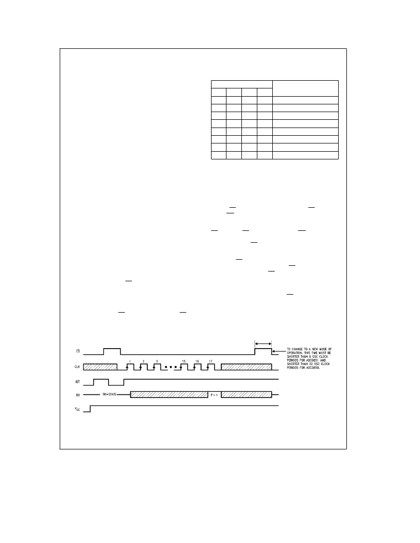
1.1 POWER FAILURE DETECTION/
INITIALIZATION AFTER POWER-UP
Upon power up, the device is automatically configured in the
watchdog mode. The status of the power flag bit, P, pro-
vides power failure indication to the microprocessor. The
timing diagram of Figure 2 shows the sequence of events.
First consider the case of initial power up. After power is
applied, CS should be brought high. Bringing CS high caus-
es the INT pin to go low, which signals the microprocessor
that a failure has occurred. The microprocessor can then
interrogate the device as to the type of failure by bringing
CS low. When CS goes low, it resets the INT pin to high and
the output data is read starting at the first rising edge of
clock (CLK) after CS has gone low. Since this is the first
read cycle after power up, the power flag bit, P, is set high
and appears at the rising edge of the seventeenth clock
cycle after CS low is detected (Figure 2). After the power
flag is read by the microprocessor, CS is taken high. Note
that the duration for which CS remains high (after the power
flag is read) must be less than eight oscillator clock periods
for ADC0851 and less than thirty-two oscillator clock peri-
ods for ADC0858. This is required to interrupt the device
from watchdog mode so that when CS goes low, the device
reads a valid data input (DI) word and configures to a new
mode.
During normal operation, the power flag bit is reset to zero
after the first ‘‘read’’ cycle and will be updated to a ‘‘1’’ only
if a power interruption occurs.
TL/H/11021–30
FIGURE 2. Read Power Flag after
Power Up ADC0851/ADC0858
17
相关PDF资料 |
PDF描述 |
|---|---|
| ADC0858CIV | 8-Bit Analog Data Acquisition and Monitoring Systems |
| ADC0881 | 8-Bit 20 MSPS Flash A/D Converter |
| ADC0881CCC | 8-Bit 20 MSPS Flash A/D Converter |
| ADC0881CCJ | 8-Bit 20 MSPS Flash A/D Converter |
| ADC0881CCN | 8-Bit 20 MSPS Flash A/D Converter |
相关代理商/技术参数 |
参数描述 |
|---|---|
| ADC0858CIV | 制造商:NSC 制造商全称:National Semiconductor 功能描述:8-Bit Analog Data Acquisition and Monitoring Systems |
| ADC0858CMJ/883 | 制造商:未知厂家 制造商全称:未知厂家 功能描述:Single-Ended Data Acquisition System |
| ADC0881 | 制造商:NSC 制造商全称:National Semiconductor 功能描述:8-Bit 20 MSPS Flash A/D Converter |
| ADC0881CCC | 制造商:NSC 制造商全称:National Semiconductor 功能描述:8-Bit 20 MSPS Flash A/D Converter |
| ADC0881CCJ | 制造商:NSC 制造商全称:National Semiconductor 功能描述:8-Bit 20 MSPS Flash A/D Converter |
发布紧急采购,3分钟左右您将得到回复。