- 您现在的位置:买卖IC网 > PDF目录16534 > ADCLK914/PCBZ (Analog Devices Inc)BOARD EVAL FOR ADCLK914 PDF资料下载
参数资料
| 型号: | ADCLK914/PCBZ |
| 厂商: | Analog Devices Inc |
| 文件页数: | 1/12页 |
| 文件大小: | 0K |
| 描述: | BOARD EVAL FOR ADCLK914 |
| 设计资源: | ADCLK9xx Eval Brd Schematics ADCLK914 Gerber File ADCLK914 BOM |
| 标准包装: | 1 |
| 主要目的: | 计时,时钟分配 |
| 已用 IC / 零件: | ADCLK914 |
| 已供物品: | 板 |
Ultrafast, SiGe, Open-Collector
HVDS Clock/Data Buffer
ADCLK914
Rev. A
Information furnished by Analog Devices is believed to be accurate and reliable. However, no
responsibilityis assumedbyAnalogDevicesforitsuse,norforanyinfringementsof patentsorother
rightsofthirdpartiesthatmayresultfromitsuse.Specificationssubjecttochangewithoutnotice.No
license is granted by implication or otherwise under any patent or patent rights of Analog Devices.
Trademarksandregisteredtrademarksarethepropertyoftheirrespectiveowners.
One Technology Way, P.O. Box 9106, Norwood, MA 02062-9106, U.S.A.
Tel: 781.329.4700
www.analog.com
Fax: 781.461.3113
2008 Analog Devices, Inc. All rights reserved.
FEATURES
7.5 GHz operating frequency
160 ps propagation delay
100 ps output rise/fall
110 fs random jitter
On-chip input terminations
Extended industrial temperature range: 40°C to +125°C
3.3 V power supply (VCC VEE)
APPLICATIONS
Clock and data signal restoration
High speed converter clocking
Broadband communications
Cellular infrastructure
High speed line receivers
ATE and high performance instrumentation
Level shifting
Threshold detection
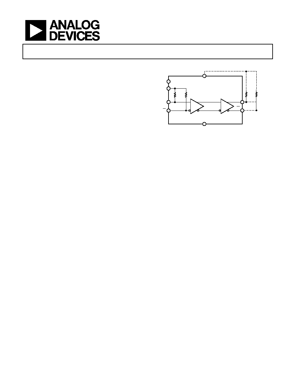
FUNCTIONAL BLOCK DIAGRAM
D
Q
VCC
VEE
VT
Q
D
Q
VCC
VEE
VT
Q
VREF
0656
1-
001
50
ADCLK914
Figure 1.
GENERAL DESCRIPTION
The ADCLK914 is an ultrafast clock/data buffer fabricated on
the Analog Devices, Inc., proprietary, complementary bipolar
(XFCB-3) silicon-germanium (SiGe) process. The ADCLK914
features high voltage differential signaling (HVDS) outputs
suitable for driving the latest Analog Devices high speed digital-
to-analog converters (DACs). The ADCLK914 has a single,
differential open-collector output.
The ADCLK914 buffer operates up to 7.5 GHz with a 160 ps
propagation delay and adds only 110 fs random jitter (RJ).
The input has a center tapped, 100 Ω, on-chip termination
resistor and accepts LVPECL, CML, CMOS, LVTTL, or LVDS
(ac-coupled only). A VREF pin is available for biasing ac-coupled
inputs.
The HVDS output stage is designed to directly drive 1.9 V each
side into 50 Ω terminated to VCC for a total differential output
swing of 3.8 V.
The ADCLK914 is available in a 16-lead LFCSP. It is specified
for operation over the extended industrial temperature range of
40°C to +125°C.
相关PDF资料 |
PDF描述 |
|---|---|
| VE-J4F-EZ-S | CONVERTER MOD DC/DC 72V 25W |
| ILC0402ER8N2K | INDUCTOR CER 8.2NH 0402 |
| AD9520-3/PCBZ | BOARD EVAL AD9520-3 |
| MCP131T-270E/TT | IC SUPERVISOR 2.63V LOW SOT-23B |
| EEU-EB2W100 | CAP ALUM 10UF 450V 20% RADIAL |
相关代理商/技术参数 |
参数描述 |
|---|---|
| ADCLK914XCPZ | 制造商:Analog Devices 功能描述:CLOCK AND TIMING IC - Rail/Tube |
| ADCLK925/PCBZ | 功能描述:BOARD EVAL FOR ADCLK925 16LFCSP RoHS:是 类别:编程器,开发系统 >> 评估演示板和套件 系列:- 标准包装:1 系列:- 主要目的:电信,线路接口单元(LIU) 嵌入式:- 已用 IC / 零件:IDT82V2081 主要属性:T1/J1/E1 LIU 次要属性:- 已供物品:板,电源,线缆,CD 其它名称:82EBV2081 |
| ADCLK925BCPZ-R2 | 功能描述:IC CLOCK/DATA BUFFER 1:2 16LFCSP RoHS:是 类别:集成电路 (IC) >> 时钟/计时 - 时钟缓冲器,驱动器 系列:SIGe 标准包装:74 系列:- 类型:扇出缓冲器(分配) 电路数:1 比率 - 输入:输出:1:10 差分 - 输入:输出:是/是 输入:HCSL, LVCMOS, LVDS, LVPECL, LVTTL 输出:HCSL,LVDS 频率 - 最大:400MHz 电源电压:3 V ~ 3.6 V 工作温度:-40°C ~ 85°C 安装类型:表面贴装 封装/外壳:32-VFQFN 裸露焊盘 供应商设备封装:32-QFN(5x5) 包装:管件 |
| ADCLK925BCPZ-R7 | 功能描述:IC CLOCK/DATA BUFFER 1:2 16LFCSP RoHS:是 类别:集成电路 (IC) >> 时钟/计时 - 时钟缓冲器,驱动器 系列:SIGe 产品培训模块:High Bandwidth Product Overview 标准包装:1,000 系列:Precision Edge® 类型:扇出缓冲器(分配) 电路数:1 比率 - 输入:输出:1:4 差分 - 输入:输出:是/是 输入:CML,LVDS,LVPECL 输出:CML 频率 - 最大:2.5GHz 电源电压:2.375 V ~ 2.625 V 工作温度:-40°C ~ 85°C 安装类型:表面贴装 封装/外壳:16-VFQFN 裸露焊盘,16-MLF? 供应商设备封装:16-MLF?(3x3) 包装:带卷 (TR) |
| ADCLK925BCPZ-TR | 制造商:Analog Devices 功能描述:1:2 ECL,,7 GBPPS CLOCK/DATA BUFFERS - Tape and Reel |
发布紧急采购,3分钟左右您将得到回复。