- 您现在的位置:买卖IC网 > PDF目录16534 > ADCLK914/PCBZ (Analog Devices Inc)BOARD EVAL FOR ADCLK914 PDF资料下载
参数资料
| 型号: | ADCLK914/PCBZ |
| 厂商: | Analog Devices Inc |
| 文件页数: | 8/12页 |
| 文件大小: | 0K |
| 描述: | BOARD EVAL FOR ADCLK914 |
| 设计资源: | ADCLK9xx Eval Brd Schematics ADCLK914 Gerber File ADCLK914 BOM |
| 标准包装: | 1 |
| 主要目的: | 计时,时钟分配 |
| 已用 IC / 零件: | ADCLK914 |
| 已供物品: | 板 |
ADCLK914
Rev. A | Page 5 of 12
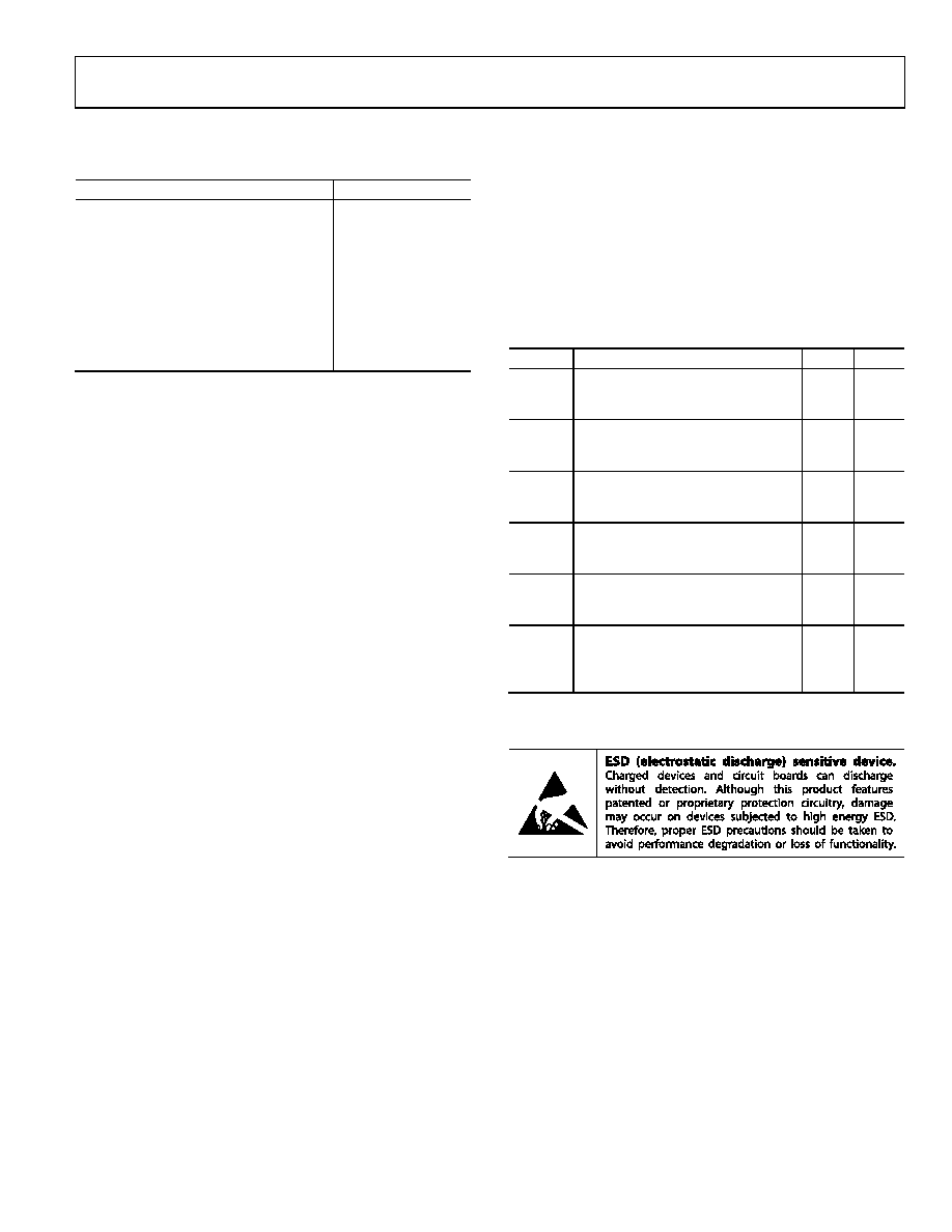
ABSOLUTE MAXIMUM RATINGS
Table 2.
Parameter
Rating
Supply Voltage (VCC to GND)
6.0 V
Input Voltage
0.5 V to VCC + 0.5 V
Maximum Output Voltage
VCC + 0.5 V
Minimum Output Voltage
VEE 0.5 V
Input Termination
±2 V
Voltage Reference
VCC VEE
Operating Temperature Range, Ambient
40°C to +125°C
Operating Temperature, Junction
150°C
Storage Temperature Range
65°C to +150°C
Stresses above those listed under Absolute Maximum Ratings
may cause permanent damage to the device. This is a stress
rating only; functional operation of the device at these or any
other conditions above those indicated in the operational
section of this specification is not implied. Exposure to absolute
maximum rating conditions for extended periods may affect
device reliability.
THERMAL PERFORMANCE
The ADCLK914 is specified for a case temperature (TCASE). To
ensure that TCASE is not exceeded, use an airflow source.
To determine the junction temperature on the application PCB
TJ = TCASE + (ΨJT × PD)
where:
TJ is the junction temperature (°C).
TCASE is the case temperature (°C) measured by the customer at
top center of package.
Ψ
JT
is determined by the values listed in Table 3.
PD is the power dissipation.
Values of θJA are provided for package comparison and PCB
design considerations. θJA can be used for a first-order
approximation of TJ by the equation
TJ = TA + (θJA × PD)
where TA is the ambient temperature (°C).
Values of θJB are provided for package comparison and PCB
design considerations.
Table 3. Thermal Parameters for ADCLK914 16-Lead LFCSP
Symbol
Value
Units
θ
JA
Junction-to-ambient thermal
resistance, 0.0 meters per sec air
flow per JEDEC JESD51-2 (still air)
78.4
°C/W
θ
JMA
Junction-to-ambient thermal
resistance, 1.0 meter per sec air flow
per JEDEC JESD51-6 (moving air)
68.5
°C/W
θ
JMA
Junction-to-ambient thermal
resistance, 2.5 m/s air flow per
JEDEC JESD51-6 (moving air)
61.4
°C/W
θ
JB
Junction-to-board thermal
resistance, 1.0 meter per sec air flow
per JEDEC JESD51-8 (moving air)
48.8
°C/W
θ
JC
Junction-to-case thermal resistance
(die-to-heatsink) per MIL-Std 883,
Method 1012.1
1.5
°C/W
Ψ
JT
Junction-to-top-of-package
characterization parameter, 0
meters per sec air flow per JEDEC
JESD51-2 (still air)
2.0
°C/W
1 Descriptions based on using a 2s2p test board.
ESD CAUTION
相关PDF资料 |
PDF描述 |
|---|---|
| VE-J4F-EZ-S | CONVERTER MOD DC/DC 72V 25W |
| ILC0402ER8N2K | INDUCTOR CER 8.2NH 0402 |
| AD9520-3/PCBZ | BOARD EVAL AD9520-3 |
| MCP131T-270E/TT | IC SUPERVISOR 2.63V LOW SOT-23B |
| EEU-EB2W100 | CAP ALUM 10UF 450V 20% RADIAL |
相关代理商/技术参数 |
参数描述 |
|---|---|
| ADCLK914XCPZ | 制造商:Analog Devices 功能描述:CLOCK AND TIMING IC - Rail/Tube |
| ADCLK925/PCBZ | 功能描述:BOARD EVAL FOR ADCLK925 16LFCSP RoHS:是 类别:编程器,开发系统 >> 评估演示板和套件 系列:- 标准包装:1 系列:- 主要目的:电信,线路接口单元(LIU) 嵌入式:- 已用 IC / 零件:IDT82V2081 主要属性:T1/J1/E1 LIU 次要属性:- 已供物品:板,电源,线缆,CD 其它名称:82EBV2081 |
| ADCLK925BCPZ-R2 | 功能描述:IC CLOCK/DATA BUFFER 1:2 16LFCSP RoHS:是 类别:集成电路 (IC) >> 时钟/计时 - 时钟缓冲器,驱动器 系列:SIGe 标准包装:74 系列:- 类型:扇出缓冲器(分配) 电路数:1 比率 - 输入:输出:1:10 差分 - 输入:输出:是/是 输入:HCSL, LVCMOS, LVDS, LVPECL, LVTTL 输出:HCSL,LVDS 频率 - 最大:400MHz 电源电压:3 V ~ 3.6 V 工作温度:-40°C ~ 85°C 安装类型:表面贴装 封装/外壳:32-VFQFN 裸露焊盘 供应商设备封装:32-QFN(5x5) 包装:管件 |
| ADCLK925BCPZ-R7 | 功能描述:IC CLOCK/DATA BUFFER 1:2 16LFCSP RoHS:是 类别:集成电路 (IC) >> 时钟/计时 - 时钟缓冲器,驱动器 系列:SIGe 产品培训模块:High Bandwidth Product Overview 标准包装:1,000 系列:Precision Edge® 类型:扇出缓冲器(分配) 电路数:1 比率 - 输入:输出:1:4 差分 - 输入:输出:是/是 输入:CML,LVDS,LVPECL 输出:CML 频率 - 最大:2.5GHz 电源电压:2.375 V ~ 2.625 V 工作温度:-40°C ~ 85°C 安装类型:表面贴装 封装/外壳:16-VFQFN 裸露焊盘,16-MLF? 供应商设备封装:16-MLF?(3x3) 包装:带卷 (TR) |
| ADCLK925BCPZ-TR | 制造商:Analog Devices 功能描述:1:2 ECL,,7 GBPPS CLOCK/DATA BUFFERS - Tape and Reel |
发布紧急采购,3分钟左右您将得到回复。