- 您现在的位置:买卖IC网 > PDF目录8761 > ADCLK944BCPZ-R2 (Analog Devices Inc)IC CLOCK BUFFER 1:4 7GHZ 16LFCSP PDF资料下载
参数资料
| 型号: | ADCLK944BCPZ-R2 |
| 厂商: | Analog Devices Inc |
| 文件页数: | 12/12页 |
| 文件大小: | 0K |
| 描述: | IC CLOCK BUFFER 1:4 7GHZ 16LFCSP |
| 标准包装: | 1 |
| 系列: | SIGe |
| 类型: | 扇出缓冲器(分配) |
| 电路数: | 1 |
| 比率 - 输入:输出: | 1:4 |
| 差分 - 输入:输出: | 是/是 |
| 输入: | CML,CMOS,LVDS,LVPECL |
| 输出: | ECL,LVPECL |
| 频率 - 最大: | 7GHz |
| 电源电压: | 2.375 V ~ 3.63 V |
| 工作温度: | -40°C ~ 85°C |
| 安装类型: | 表面贴装 |
| 封装/外壳: | 16-WFQFN 裸露焊盘,CSP |
| 供应商设备封装: | 16-LFCSP-WQ(3x3) |
| 包装: | 标准包装 |
| 其它名称: | ADCLK944BCPZ-R2DKR |
ADCLK944
Rev. 0 | Page 9 of 12
THEORY OF OPERATION
CLOCK INPUTS
The ADCLK944 accepts a differential clock input and distrib-
utes it to all four LVPECL outputs. The maximum specified
frequency is the point at which the output voltage swing is 50%
of the standard LVPECL swing (see Figure 4).
The device has a differential input equipped with center-tapped,
differential, 100 Ω on-chip termination resistors. The input can
accept dc-coupled LVPECL, CML, 3.3 V CMOS (single-ended,
3.3 V operation only), and ac-coupled 1.8 V CMOS, LVDS, and
LVPECL inputs. A VREF pin is available for biasing ac-coupled
Maintain the differential input voltage swing from approxi-
mately 400 mV p-p to no more than 3.4 V p-p. See Figure 18
through Figure 21 for various clock input termination schemes.
Output jitter performance is significantly degraded by an input
slew rate below 1 V/ns, as shown in Figure 11. The ADCLK944
is specifically designed to minimize added random jitter over a
wide input slew rate range. Whenever possible, clamp excessively
large input signals with fast Schottky diodes because attenuators
reduce the slew rate. Input signal runs of more than a few centi-
meters should be over low loss dielectrics or cables with good
high frequency characteristics.
CLOCK OUTPUTS
The specified performance necessitates using proper transmis-
sion line terminations. The LVPECL outputs of the ADCLK944
are designed to directly drive 800 mV into a 50 Ω cable or into
microstrip/stripline transmission lines terminated with 50 Ω
output stage is shown in Figure 12. The outputs are designed
for best transmission line matching. If high speed signals must
be routed more than a centimeter, either the microstrip or the
stripline technique is required to ensure proper transition times
and to prevent excessive output ringing and pulse-width-dependent
propagation delay dispersion.
VEE
VCC
Q
08
77
0-
0
1
3
Figure 12. Simplified Schematic Diagram
of the LVPECL Output Stage
termination schemes. When dc-coupled, VCC of the receiving
buffer should match VS_DRV.
ADCLK944
VS_DRV
VCC = VS_DRV
Z0 = 50
LVPECL
50
VCC – 2V
50
08
77
0-
0
1
4
Z0 = 50
Figure 13. DC-Coupled, 3.3 V LVPECL
Thevenin-equivalent termination uses a resistor network to provide
50 Ω termination to a dc voltage that is below VOL of the LVPECL
driver. In this case, VS_DRV on the ADCLK944 should equal
VCC of the receiving buffer. Although the resistor combination
shown in Figure 14 results in a dc bias point of VS_DRV 2 V,
the actual common-mode voltage is VS_DRV 1.3 V because
there is additional current flowing from the ADCLK944 LVPECL
driver through the pull-down resistor.
VS_DRV
50
50
SINGLE-ENDED
(NOT COUPLED)
VS_DRV
ADCLK944
VCC
LVPECL
127
127
83
83
87
70
-01
5
0
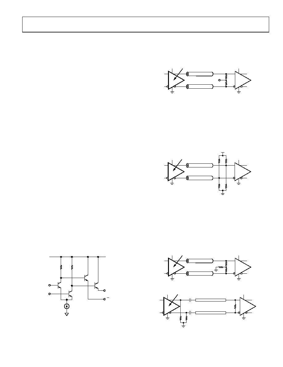
Figure 14. DC-Coupled, 3.3 V LVPECL Far-End Thevenin Termination
LVPECL Y-termination (see Figure 15) is an elegant termination
scheme that uses the fewest components and offers both odd-
and even-mode impedance matching. Even-mode impedance
matching is an important consideration for closely coupled trans-
mission lines at high frequencies. Its main drawback is that it offers
limited flexibility for varying the drive strength of the emitter-
follower LVPECL driver. This can be an important consideration
when driving long trace lengths but is usually not an issue.
ADCLK944
VS_DRV
VCC = VS_DRV
Z0 = 50
LVPECL
50
50
50
87
70-
0
16
Z0 = 50
0
Figure 15. DC-Coupled, 3.3 V LVPECL Y-Termination
A
VS_DRV
100
DIFFERENTIAL
(COUPLED)
TRANSMISSION LINE
VCC
LVPECL
100
0.1nF
DCLK944
200
200
08
77
0-
01
7
Figure 16. AC-Coupled LVPECL with Parallel Transmission Line
相关PDF资料 |
PDF描述 |
|---|---|
| D38999/26MJ7SALC | CONN HSG PLUG 99POS STRGHT SCKT |
| D38999/26JJ8AC | CONN HSG PLUG 8POS STRGHT PINS |
| D38999/26JJ8AA | CONN HSG PLUG 8POS STRGHT PINS |
| D38999/26JJ8AN | CONN HSG PLUG 8POS STRGHT PINS |
| D38999/26MJ8PNLC | CONN HSG PLUG 8POS STRGHT PINS |
相关代理商/技术参数 |
参数描述 |
|---|---|
| ADCLK944BCPZ-R7 | 功能描述:IC CLOCK BUFFER 1:4 7GHZ 16LFCSP RoHS:是 类别:集成电路 (IC) >> 时钟/计时 - 时钟缓冲器,驱动器 系列:SIGe 标准包装:74 系列:- 类型:扇出缓冲器(分配) 电路数:1 比率 - 输入:输出:1:10 差分 - 输入:输出:是/是 输入:HCSL, LVCMOS, LVDS, LVPECL, LVTTL 输出:HCSL,LVDS 频率 - 最大:400MHz 电源电压:3 V ~ 3.6 V 工作温度:-40°C ~ 85°C 安装类型:表面贴装 封装/外壳:32-VFQFN 裸露焊盘 供应商设备封装:32-QFN(5x5) 包装:管件 |
| ADCLK944BCPZ-WP | 功能描述:IC CLOCK BUFFER 1:4 7GHZ 16LFCSP RoHS:是 类别:集成电路 (IC) >> 时钟/计时 - 时钟缓冲器,驱动器 系列:SIGe 产品培训模块:High Bandwidth Product Overview 标准包装:1,000 系列:Precision Edge® 类型:扇出缓冲器(分配) 电路数:1 比率 - 输入:输出:1:4 差分 - 输入:输出:是/是 输入:CML,LVDS,LVPECL 输出:CML 频率 - 最大:2.5GHz 电源电压:2.375 V ~ 2.625 V 工作温度:-40°C ~ 85°C 安装类型:表面贴装 封装/外壳:16-VFQFN 裸露焊盘,16-MLF? 供应商设备封装:16-MLF?(3x3) 包装:带卷 (TR) |
| ADCLK946 | 制造商:AD 制造商全称:Analog Devices 功能描述:Six LVPECL Outputs, SiGe Clock Fanout Buffer |
| ADCLK946/PCBZ | 功能描述:KIT EVAL CLK BUFF ADCLK946 RoHS:是 类别:编程器,开发系统 >> 评估演示板和套件 系列:- 标准包装:1 系列:- 主要目的:电信,线路接口单元(LIU) 嵌入式:- 已用 IC / 零件:IDT82V2081 主要属性:T1/J1/E1 LIU 次要属性:- 已供物品:板,电源,线缆,CD 其它名称:82EBV2081 |
| ADCLK946BCPZ | 功能描述:IC CLK BUFFER 1:6 4.8GHZ 24LFCSP RoHS:是 类别:集成电路 (IC) >> 时钟/计时 - 时钟缓冲器,驱动器 系列:SIGe 标准包装:74 系列:- 类型:扇出缓冲器(分配) 电路数:1 比率 - 输入:输出:1:10 差分 - 输入:输出:是/是 输入:HCSL, LVCMOS, LVDS, LVPECL, LVTTL 输出:HCSL,LVDS 频率 - 最大:400MHz 电源电压:3 V ~ 3.6 V 工作温度:-40°C ~ 85°C 安装类型:表面贴装 封装/外壳:32-VFQFN 裸露焊盘 供应商设备封装:32-QFN(5x5) 包装:管件 |
发布紧急采购,3分钟左右您将得到回复。