- 您现在的位置:买卖IC网 > PDF目录16534 > ADCLK946/PCBZ (Analog Devices Inc)KIT EVAL CLK BUFF ADCLK946 PDF资料下载
参数资料
| 型号: | ADCLK946/PCBZ |
| 厂商: | Analog Devices Inc |
| 文件页数: | 2/12页 |
| 文件大小: | 0K |
| 描述: | KIT EVAL CLK BUFF ADCLK946 |
| 设计资源: | ADCLK946 Schematic ADCLK946 Gerber File ADCLK946 BOM |
| 标准包装: | 1 |
| 主要目的: | 计时,时钟缓冲器 / 驱动器 / 接收器 / 变换器 |
| 嵌入式: | 否 |
| 已用 IC / 零件: | ADCLK946 |
| 主要属性: | 1 输入,6 输出 |
| 次要属性: | LVPECL 输出逻辑 |
| 已供物品: | 板 |
ADCLK946
Rev. A | Page 10 of 12
PCB LAYOUT CONSIDERATIONS
The ADCLK946 buffer is designed for very high speed
applications. Consequently, high speed design techniques must
be used to achieve the specified performance. It is critically
important to use low impedance supply planes for both the
negative supply (VEE) and the positive supply (VCC) planes as
part of a multilayer board. Providing the lowest inductance
return path for switching currents ensures the best possible
performance in the target application.
The following references to the ground plane assume that
the VEE power plane is grounded for LVPECL operation.
Note that, for ECL operation, the VCC power plane becomes
the ground plane.
It is also important to adequately bypass the input and output
supplies. Place a 1 F electrolytic bypass capacitor within several
inches of each VCC power supply pin to the ground plane. In
addition, place multiple high quality 0.001 F bypass capacitors
as close as possible to each of the VCC supply pins, and connect
the capacitors to the ground plane with redundant vias.
Carefully select high frequency bypass capacitors for minimum
inductance and ESR. To improve the effectiveness of the bypass
at high frequencies, minimize parasitic layout inductance. Also,
avoid discontinuities along input and output transmission lines
that can affect jitter performance.
In a 50 environment, input and output matching have a
significant impact on performance. The buffer provides internal
50 termination resistors for both CLK and CLK inputs.
Normally, the return side is connected to the reference pin that is
provided. Carefully bypass the termination potential using
ceramic capacitors to prevent undesired aberrations on the
input signal due to parasitic inductance in the termination
return path. If the inputs are dc-coupled to a source, take care to
ensure that the pins are within the rated input differential and
common-mode ranges.
If the return is floated, the device exhibits a 100 Ω cross-
termination, but the source must then control the common-
mode voltage and supply the input bias currents.
There are ESD/clamp diodes between the input pins to prevent
the application from developing excessive offsets to the input
transistors. ESD diodes are not optimized for best ac perfor-
mance. When a clamp is required, it is recommended that
appropriate external diodes be used.
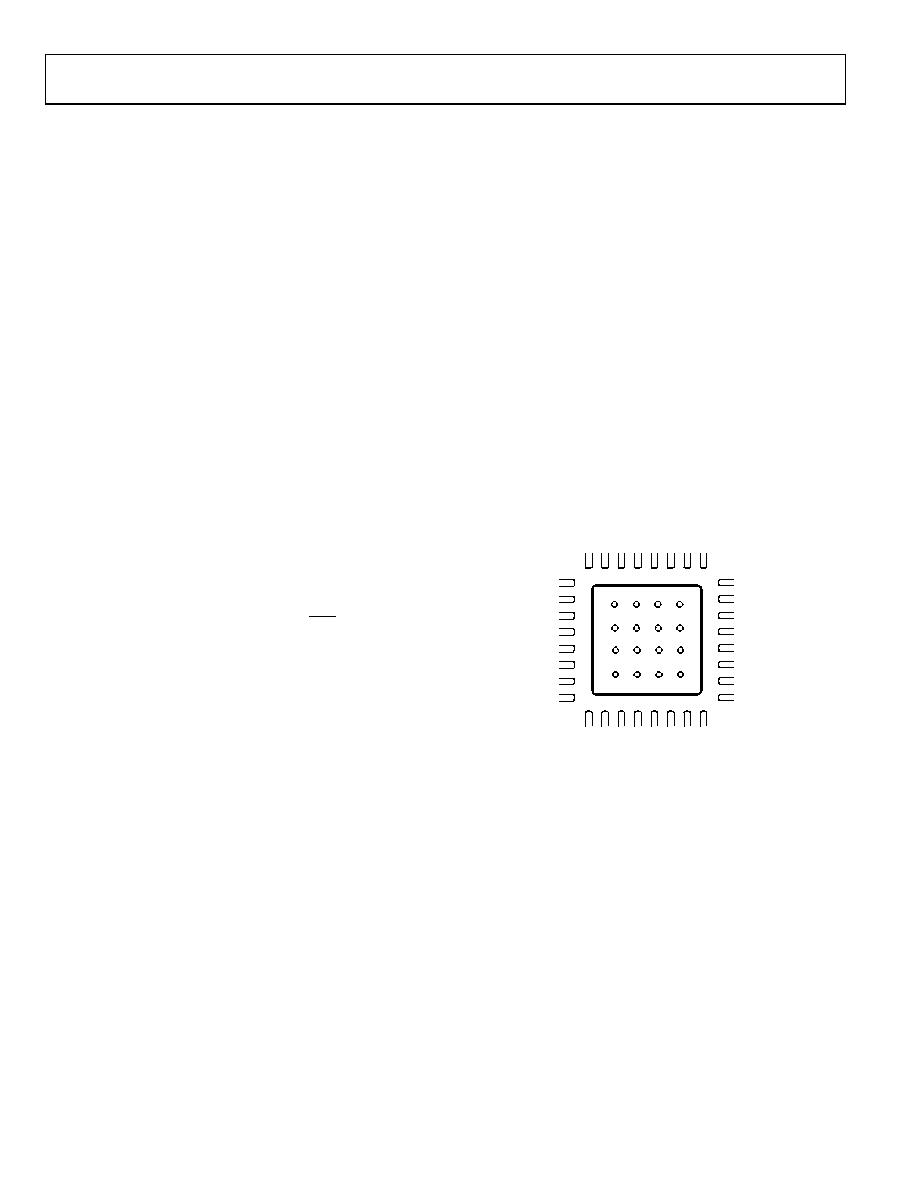
Exposed Metal Paddle
The exposed metal paddle on the ADCLK946 package is both
an electrical connection and a thermal enhancement. For the
device to function properly, the paddle must be properly
attached to the VEE pin.
When properly mounted, the ADCLK946 also dissipates heat
through its exposed paddle. The PCB acts as a heat sink for the
ADCLK946. The PCB attachment must provide a good thermal
path to a larger heat dissipation area. This requires a grid of vias
The ADCLK946 evaluation board (ADCLK946/PCBZ)
provides an example of how to attach the part to the PCB.
VIAS TO VEE POWER
PLANE
08053-
018
Figure 18. PCB Land for Attaching Exposed Paddle
相关PDF资料 |
PDF描述 |
|---|---|
| A2MXS-3436M | ADM34S/AE34M/X |
| FCBP110LD1L05S | KIT 5M LASERWIRE SFP+ |
| AD9522-3/PCBZ | BOARD EVAL FOR AD9522-3 CLK GEN |
| FCBP110LD1L03S | KIT 3M LASERWIRE SFP+ |
| VE-J4D-EZ-S | CONVERTER MOD DC/DC 85V 25W |
相关代理商/技术参数 |
参数描述 |
|---|---|
| ADCLK948 | 制造商:AD 制造商全称:Analog Devices 功能描述:Two Selectable Inputs, 8 LVPECL Outputs, SiGe Clock Fanout Buffer |
| ADCLK948/PCBZ | 功能描述:BOARD EVALUATION FOR ADCLK948 RoHS:是 类别:编程器,开发系统 >> 评估演示板和套件 系列:SIGe 标准包装:1 系列:PSoC® 主要目的:电源管理,热管理 嵌入式:- 已用 IC / 零件:- 主要属性:- 次要属性:- 已供物品:板,CD,电源 |
| ADCLK948BCPZ | 功能描述:IC CLOCK BUFFER MUX 2:8 32-LFCSP RoHS:是 类别:集成电路 (IC) >> 时钟/计时 - 时钟缓冲器,驱动器 系列:SIGe 产品培训模块:High Bandwidth Product Overview 标准包装:1,000 系列:Precision Edge® 类型:扇出缓冲器(分配) 电路数:1 比率 - 输入:输出:1:4 差分 - 输入:输出:是/是 输入:CML,LVDS,LVPECL 输出:CML 频率 - 最大:2.5GHz 电源电压:2.375 V ~ 2.625 V 工作温度:-40°C ~ 85°C 安装类型:表面贴装 封装/外壳:16-VFQFN 裸露焊盘,16-MLF? 供应商设备封装:16-MLF?(3x3) 包装:带卷 (TR) |
| ADCLK948BCPZ | 制造商:Analog Devices 功能描述:CLOCK FANOUT BUFFER, 4.8GHZ, LFCSP-32 |
| ADCLK948BCPZ-REEL7 | 功能描述:IC CLOCK BUFFER MUX 2:8 32-LFCSP RoHS:是 类别:集成电路 (IC) >> 时钟/计时 - 时钟缓冲器,驱动器 系列:SIGe 标准包装:74 系列:- 类型:扇出缓冲器(分配) 电路数:1 比率 - 输入:输出:1:10 差分 - 输入:输出:是/是 输入:HCSL, LVCMOS, LVDS, LVPECL, LVTTL 输出:HCSL,LVDS 频率 - 最大:400MHz 电源电压:3 V ~ 3.6 V 工作温度:-40°C ~ 85°C 安装类型:表面贴装 封装/外壳:32-VFQFN 裸露焊盘 供应商设备封装:32-QFN(5x5) 包装:管件 |
发布紧急采购,3分钟左右您将得到回复。