参数资料
| 型号: | ADCMP566BCPZ |
| 厂商: | Analog Devices Inc |
| 文件页数: | 15/16页 |
| 文件大小: | 0K |
| 描述: | IC COMP DUAL ULTRA-FAST 32LFCSP |
| 标准包装: | 1 |
| 类型: | 带锁销 |
| 元件数: | 2 |
| 输出类型: | 补充型,差分,ECL,开路发射极 |
| 电压 - 电源,单路/双路(±): | ±4.75 V ~ 5.25 V |
| 电压 - 输入偏移(最小值): | 5mV @ -5.2V,5V |
| 电流 - 输入偏压(最小值): | 42µA @ -5.2V,5V |
| 电流 - 输出(标准): | 30mA |
| 电流 - 静态(最大值): | 18mA,85mA |
| CMRR, PSRR(标准): | 69dB CMRR |
| 传输延迟(最大): | 0.29ns |
| 磁滞: | ±1mV |
| 工作温度: | -40°C ~ 85°C |
| 封装/外壳: | 32-VFQFN 裸露焊盘,CSP |
| 安装类型: | 表面贴装 |
| 包装: | 托盘 |
| 产品目录页面: | 764 (CN2011-ZH PDF) |
| 配用: | EVAL-ADCMP566BCPZ-ND - BOARD EVALUATION ADCMP566BPZ |
ADCMP566
Rev. 0 | Page 8 of 16
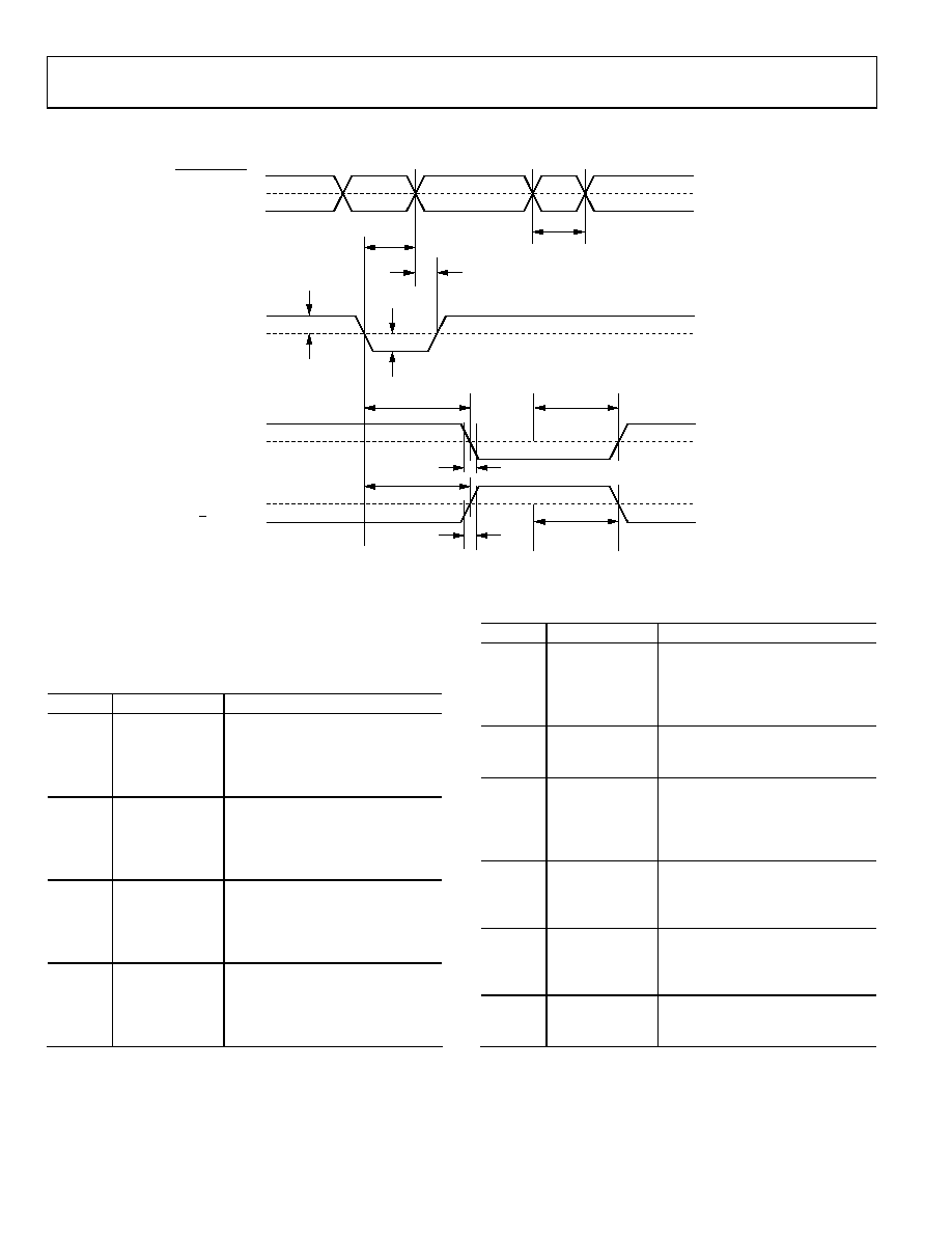
TIMING INFORMATION
50%
VREF ± VOS
50%
DIFFERENTIAL
INPUT VOLTAGE
LATCH ENABLE
Q OUTPUT
LATCH ENABLE
tH
tPDL
tPDH
tPLOH
tPLOL
tR
tF
VIN
VOD
tS
tPL
03633-0-003
Figure 3. System Timing Diagram
The timing diagram in Figure 3 shows the ADCMP566 compare
and latch features. Table 4 describes the terms in the diagram.
Table 4. Timing Descriptions
Symbol
Timing
Description
tPDH
Input to output
high delay
Propagation delay measured from
the time the input signal crosses
the reference (± the input offset
voltage) to the 50% point of an
output low-to-high transition
tPDL
Input to output
low delay
Propagation delay measured from
the time the input signal crosses
the reference (± the input offset
voltage) to the 50% point of an
output high-to-low transition
tPLOH
Latch enable
to output high
delay
Propagation delay measured from
the 50% point of the Latch Enable
signal low-to-high transition to
the 50% point of an output low-
to-high transition
tPLOL
Latch enable
to output low
delay
Propagation delay measured from
the 50% point of the Latch Enable
signal low-to-high transition to
the 50% point of an output high-
to-low transition
Symbol
Timing
Description
tH
Minimum
hold time
Minimum time after the negative
transition of the Latch Enable
signal that the input signal must
remain unchanged to be acquired
and held at the outputs
tPL
Minimum
latch enable
pulsewidth
Minimum time that the Latch
Enable signal must be high to
acquire an input signal change
tS
Minimum
setup time
Minimum time before the
negative transition of the Latch
Enable signal that an input signal
change must be present to be
acquired and held at the outputs
tR
Output rise
time
Amount of time required to
transition from a low to a high
output as measured at the 20%
and 80% points
tF
Output fall
time
Amount of time required to
transition from a high to a low
output as measured at the 20%
and 80% points
VOD
Voltage
overdrive
Difference between the
differential input and reference
input voltages
相关PDF资料 |
PDF描述 |
|---|---|
| ADCMP567BCPZ | IC COMP DUAL ULTRA-FAST 32LFCSP |
| ADCMP573BCPZ-WP | IC COMPARATOR PECL 3.3-5 16LFCSP |
| ADCMP580BCPZ-R2 | IC COMPARATOR CML UFAST 16-LFCSP |
| ADCMP601BKSZ-R2 | IC COMP TTL/CMOS 1CHAN SC70-6 |
| ADCMP603BCPZ-WP | IC COMP TTL/CMOS 1CHAN 12-LFCSP |
相关代理商/技术参数 |
参数描述 |
|---|---|
| ADCMP567 | 制造商:AD 制造商全称:Analog Devices 功能描述:Dual Ultrafast Voltage Comparator |
| ADCMP567BCP | 制造商:Analog Devices 功能描述:Comparator Dual -5.45V/5.25V 32-Pin LFCSP EP 制造商:Analog Devices 功能描述:IC COMPARATOR HIGH SPEED |
| ADCMP567BCPZ | 功能描述:IC COMP DUAL ULTRA-FAST 32LFCSP RoHS:是 类别:集成电路 (IC) >> 线性 - 比较器 系列:- 标准包装:1 系列:- 类型:通用 元件数:1 输出类型:CMOS,开路集电极,TTL 电压 - 电源,单路/双路(±):2.7 V ~ 5.5 V 电压 - 输入偏移(最小值):7mV @ 5V 电流 - 输入偏压(最小值):0.25µA @ 5V 电流 - 输出(标准):84mA @ 5V 电流 - 静态(最大值):120µA CMRR, PSRR(标准):- 传输延迟(最大):600ns 磁滞:- 工作温度:-40°C ~ 85°C 封装/外壳:SC-74A,SOT-753 安装类型:表面贴装 包装:剪切带 (CT) 产品目录页面:1268 (CN2011-ZH PDF) 其它名称:*LMV331M5*LMV331M5/NOPBLMV331M5CT |
| ADCMP572 | 制造商:AD 制造商全称:Analog Devices 功能描述:Ultrafast 3.3 V Single-Supply Comparators |
| ADCMP572_05 | 制造商:AD 制造商全称:Analog Devices 功能描述:Ultrafast 3.3 V/5 V Single-Supply SiGe Comparators |
发布紧急采购,3分钟左右您将得到回复。