- 您现在的位置:买卖IC网 > PDF目录10735 > ADCMP581BCPZ-WP (Analog Devices Inc)IC COMPARATOR ECL UFAST 16-LFCSP PDF资料下载
参数资料
| 型号: | ADCMP581BCPZ-WP |
| 厂商: | Analog Devices Inc |
| 文件页数: | 3/16页 |
| 文件大小: | 0K |
| 描述: | IC COMPARATOR ECL UFAST 16-LFCSP |
| 标准包装: | 50 |
| 类型: | 带锁销 |
| 元件数: | 1 |
| 输出类型: | 补充型,ECL |
| 电压 - 电源,单路/双路(±): | ±4.5 V ~ 5.5 V |
| 电压 - 输入偏移(最小值): | 10mV @ ±5V |
| 电流 - 输入偏压(最小值): | 30µA @ ±5V |
| 电流 - 输出(标准): | 44mA @ 5V |
| 电流 - 静态(最大值): | 8mA |
| CMRR, PSRR(标准): | 60dB CMRR,75dB PSRR |
| 传输延迟(最大): | 0.18ns |
| 磁滞: | 1mV |
| 工作温度: | -40°C ~ 125°C |
| 封装/外壳: | 16-VFQFN 裸露焊盘,CSP |
| 安装类型: | 表面贴装 |
| 包装: | 托盘 - 晶粒 |
| 配用: | EVAL-ADCMP581BCPZ-ND - BOARD EVALUATION ADCMP581BCP |
ADCMP580/ADCMP581/ADCMP582
Rev. A | Page 11 of 16
APPLICATION INFORMATION
POWER/GROUND LAYOUT AND BYPASSING
The ADCMP58x family of comparators is designed for very
high speed applications. Consequently, high speed design
techniques must be used to achieve the specified performance.
It is critically important to use low impedance supply planes,
particularly for the negative supply (VEE), the output supply
plane (VCCO), and the ground plane (GND). Individual supply
planes are recommended as part of a multilayer board. Provid-
ing the lowest inductance return path for the switching currents
ensures the best possible performance in the target application.
It is also important to adequately bypass the input and output
supplies. A 1 μF electrolytic bypass capacitor should be placed
within several inches of each power supply pin to ground. In
addition, multiple high quality 0.1 μF bypass capacitors should
be placed as close as possible to each of the VEE, VCCI, and VCCO
supply pins and should be connected to the GND plane with
redundant vias. High frequency bypass capacitors should be
carefully selected for minimum inductance and ESR. Parasitic
layout inductance should be strictly avoided to maximize the
effectiveness of the bypass at high frequencies.
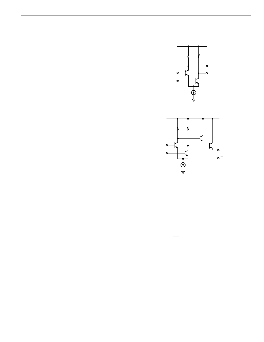
ADCMP58x FAMILY OF OUTPUT STAGES
Specified propagation delay dispersion performance is achieved
by using proper transmission line terminations. The outputs of
the ADCMP580 family comparators are designed to directly
drive 400 mV into 50 Ω cable or microstrip/stripline transmis-
sion lines terminated with 50 Ω referenced to the proper return.
The CML output stage for the ADCMP580 is shown in the
simplified schematic diagram in Figure 24. Each output is
back-terminated with 50 Ω for best transmission line matching.
The outputs of the ADCMP581/ADCMP582 are illustrated in
Figure 25; they should be terminated to 2 V for ECL outputs of
ADCMP581 and VCCO 2 V for PECL outputs of ADCMP582.
As an alternative, Thevenin equivalent termination networks
can also be used. If these high speed signals must be routed
more than a centimeter, either microstrip or stripline techniques
are required to ensure proper transition times and to prevent
excessive output ringing and pulse width-dependent propagation
delay dispersion.
Q
16mA
50
Q
GND
VEE
046
72
-02
4
Figure 24. Simplified Schematic Diagram of the ADCMP580 CML Output Stage
GND/VCCO
VEE
Q
04
67
2-
0
25
Figure 25. Simplified Schematic Diagram of the
ADCMP581/ADCMP582 ECL/PECL Output Stage
USING/DISABLING THE LATCH FEATURE
The latch inputs (LE/LE) are active low for latch mode and are
internally terminated with 50 Ω resistors to the VTT pin. When
using the ADCMP580, VTT should be connected to ground.
When using the ADCMP581, VTT should be connected to 2 V.
When using the ADCMP582, VTT should be connected externally
to VCCO 2 V, preferably with its own low inductance plane.
When using the ADCMP580, the latch function can be disabled
by connecting the LE pin to VEE with an external pull-down
resistor and by leaving the LE pin to ground. To prevent excessive
power dissipation, the resistor should be 1 kΩ for the ADCMP580.
When using the ADCMP581 comparators, the latch can be
disabled by connecting the LE pin to VEE with an external 750 Ω
resistor and leaving the LE pin connected to 2 V. The idea is to
create an approximate 0.5 V offset using the internal resistor as
half of the voltage divider. The VTT pin should be connected as
recommended.
相关PDF资料 |
PDF描述 |
|---|---|
| ADCMP582BCPZ-WP | IC COMPARATOR PECL UFAST 16LFCSP |
| ADCMP572BCPZ-WP | IC COMPARATOR CML 3.3-5V 16LFCSP |
| VE-J4V-MY-F4 | CONVERTER MOD DC/DC 5.8V 50W |
| VI-JNW-MY-F2 | CONVERTER MOD DC/DC 5.5V 50W |
| VE-2WN-MY-B1 | CONVERTER MOD DC/DC 18.5V 50W |
相关代理商/技术参数 |
参数描述 |
|---|---|
| ADCMP582 | 制造商:AD 制造商全称:Analog Devices 功能描述:Ultrafast SiGe Voltage Comparator |
| ADCMP582BCP | 制造商:Analog Devices 功能描述:COMPARATOR SGL 5.5V 16LFCSP EP - Bulk |
| ADCMP582BCP-R2 | 制造商:Analog Devices 功能描述:Comparator Single ±5.5V 16-Pin LFCSP EP T/R 制造商:Rochester Electronics LLC 功能描述:DUAL SUPPLY, PECL ON XFCB3.0 - Bulk |
| ADCMP582BCP-RL7 | 制造商:Analog Devices 功能描述:Comparator Single ±5.5V 16-Pin LFCSP EP T/R |
| ADCMP582BCP-WP | 制造商:Analog Devices 功能描述:Comparator Single ±5.5V 16-Pin LFCSP EP 制造商:Analog Devices 功能描述:IC SEMICONDUCTOR ((NS)) |
发布紧急采购,3分钟左右您将得到回复。