- 您现在的位置:买卖IC网 > PDF目录10791 > ADCMP582BCPZ-R2 (Analog Devices Inc)IC COMPARATOR PECL UFAST 16LFCSP PDF资料下载
参数资料
| 型号: | ADCMP582BCPZ-R2 |
| 厂商: | Analog Devices Inc |
| 文件页数: | 14/16页 |
| 文件大小: | 0K |
| 描述: | IC COMPARATOR PECL UFAST 16LFCSP |
| 标准包装: | 1 |
| 类型: | 带锁销 |
| 元件数: | 1 |
| 输出类型: | 补充型,PECL |
| 电压 - 电源,单路/双路(±): | ±4.5 V ~ 5.5 V |
| 电压 - 输入偏移(最小值): | 10mV @ ±5V |
| 电流 - 输入偏压(最小值): | 30µA @ ±5V |
| 电流 - 输出(标准): | 44mA @ 5V |
| 电流 - 静态(最大值): | 8mA |
| CMRR, PSRR(标准): | 60dB CMRR,75dB PSRR |
| 传输延迟(最大): | 0.18ns |
| 磁滞: | 1mV |
| 工作温度: | -40°C ~ 125°C |
| 封装/外壳: | 16-VFQFN 裸露焊盘,CSP |
| 安装类型: | 表面贴装 |
| 包装: | 标准包装 |
| 产品目录页面: | 765 (CN2011-ZH PDF) |
| 配用: | EVAL-ADCMP582BCPZ-ND - BOARD EVALUATION ADCMP582BCP |
| 其它名称: | ADCMP582BCPZ-R2DKR |
ADCMP580/ADCMP581/ADCMP582
Rev. A | Page 7 of 16
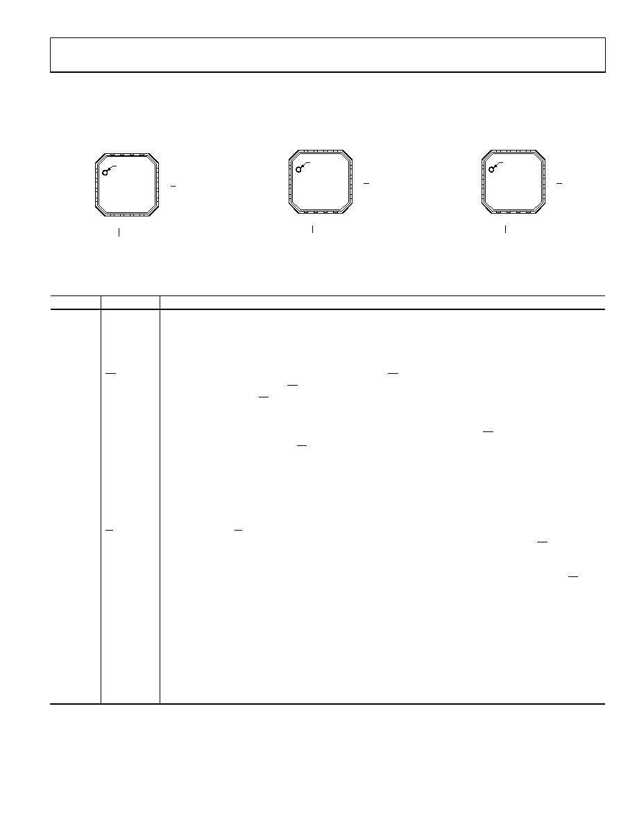
PIN CONFIGURATIONS AND FUNCTION DESCRIPTIONS
Q
LE
PIN 1
INDICATOR
1
VTP
2
VP
3
VN
4
VTN
11 Q
12 GND
10
9GND
5
V
C
I
6
7
L
E
8
V
T
15
G
N
D
16
V
C
I
14
H
Y
S
13
V
E
ADCMP580
TOP VIEW
(Not to Scale)
0
46
72
-00
3
Figure 3. ADCMP580 Pin Configuration
Q
LE
PIN 1
INDICATOR
1
VTP
2
VP
3
VN
4
VTN
11 Q
12 GND
10
9GND
5
V
C
I
6
7
L
E
8
V
T
15
G
N
D
16
V
C
I
14
H
Y
S
13
V
E
ADCMP581
TOP VIEW
(Not to Scale)
0
46
72
-00
4
Figure 4. ADCMP581 Pin Configuration
Q
LE
PIN 1
INDICATOR
1
VTP
2
VP
3
VN
4
VTN
11 Q
12 VCCO
10
9VCCO
5
V
C
I
6
7
L
E
8
V
T
15
G
N
D
16
V
C
I
14
H
Y
S
13
V
E
ADCMP582
TOP VIEW
(Not to Scale)
0
46
72
-00
5
Figure 5. ADCMP582 Pin Configuration
Table 4. Pin Function Descriptions
Pin No.
Mnemonic
Description
1
VTP
Termination Resistor Return Pin for VP Input.
2
VP
Noninverting Analog Input.
3
VN
Inverting Analog Input.
4
VTN
Termination Resistor Return Pin for VN Input.
5, 16
VCCI
Positive Supply Voltage.
6
LE
Latch Enable Input Pin, Inverting Side. In compare mode (LE = low), the output tracks changes at the input of
the comparator. In latch mode (LE = high), the output reflects the input state just prior to the comparator being
placed into latch mode. LE must be driven in complement with LE.
7
LE
Latch Enable Input Pin, Noninverting Side. In compare mode (LE = high), the output tracks changes at the
input of the comparator. In latch mode (LE = low), the output reflects the input state just prior to the
comparator being placed into latch mode. LE must be driven in complement with LE.
8
VTT
Termination Return Pin for the LE/LE Input Pins.
For the ADCMP580 (CML output stage), this pin should be connected to the GND ground.
For the ADCMP581 (ECL output stage), this pin should be connected to the –2 V termination potential.
For the ADCMP582 (PECL output stage), this pin should be connected to the VCCO – 2 V termination potential.
9, 12
GND/VCCO
Digital Ground Pin/Positive Logic Power Supply Terminal.
For the ADCMP580/ADCMP581, this pin should be connected to the GND pin.
For the ADCMP582, this pin should be connected to the positive logic power VCCO supply.
10
Q
Inverting Output. Q is logic low if the analog voltage at the noninverting input, VP, is greater than the analog
voltage at the inverting input, VN, provided that the comparator is in compare mode. See the LE/LE descriptions
(Pin 6 to Pin 7) for more information.
11
Q
Noninverting Output. Q is logic high if the analog voltage at the noninverting input, VP, is greater than the
analog voltage at the inverting input, VN, provided that the comparator is in compare mode. See the LE/LE
descriptions (Pin 6 to Pin 7) for more information.
13
VEE
Negative Power Supply.
14
HYS
Hysteresis Control. Leave this pin disconnected for zero hysteresis. Connect this pin to the VEE supply with a
suitably sized resistor to add the desired amount of hysteresis. Refer to Figure 9 for proper sizing of the HYS
hysteresis control resistor.
15
GND
Analog Ground.
Heat Sink
Paddle
N/C
The metallic back surface of the package is not electrically connected to any part of the circuit. It can be left
floating for optimal electrical isolation between the package handle and the substrate of the die. It can also
be soldered to the application board if improved thermal and/or mechanical stability is desired. Exposed metal
at package corners is connected to the heat sink paddle.
相关PDF资料 |
PDF描述 |
|---|---|
| LTC1519CS#PBF | IC LINE RCVR RS485 QUAD 16-SOIC |
| VI-JTM-MY-S | CONVERTER MOD DC/DC 10V 50W |
| LTC1348IG#PBF | IC TXRX 3.3V/5V RS232 28-SSOP |
| LTC1426CS8#PBF | IC PWM D/A CONV 6BIT DUAL 8-SOIC |
| VI-J5N-MY-S | CONVERTER MOD DC/DC 18.5V 50W |
相关代理商/技术参数 |
参数描述 |
|---|---|
| ADCMP582BCPZ-RL7 | 功能描述:IC COMPARATOR PECL UFAST 16LFCSP RoHS:是 类别:集成电路 (IC) >> 线性 - 比较器 系列:- 产品培训模块:Lead (SnPb) Finish for COTS Obsolescence Mitigation Program 标准包装:2,500 系列:- 类型:通用 元件数:1 输出类型:CMOS,推挽式,满摆幅,TTL 电压 - 电源,单路/双路(±):2.5 V ~ 5.5 V,±1.25 V ~ 2.75 V 电压 - 输入偏移(最小值):5mV @ 5.5V 电流 - 输入偏压(最小值):1pA @ 5.5V 电流 - 输出(标准):- 电流 - 静态(最大值):24µA CMRR, PSRR(标准):80dB CMRR,80dB PSRR 传输延迟(最大):450ns 磁滞:±3mV 工作温度:-40°C ~ 85°C 封装/外壳:6-WFBGA,CSPBGA 安装类型:表面贴装 包装:管件 其它名称:Q3554586 |
| ADCMP582BCPZ-WP | 功能描述:IC COMPARATOR PECL UFAST 16LFCSP RoHS:是 类别:集成电路 (IC) >> 线性 - 比较器 系列:- 产品培训模块:Lead (SnPb) Finish for COTS Obsolescence Mitigation Program 标准包装:50 系列:- 类型:带电压基准 元件数:4 输出类型:开路漏极 电压 - 电源,单路/双路(±):2.5 V ~ 11 V,±1.25 V ~ 5.5 V 电压 - 输入偏移(最小值):10mV @ 5V 电流 - 输入偏压(最小值):- 电流 - 输出(标准):0.015mA @ 5V 电流 - 静态(最大值):8.5µA CMRR, PSRR(标准):80dB CMRR,80dB PSRR 传输延迟(最大):- 磁滞:- 工作温度:0°C ~ 70°C 封装/外壳:16-SOIC(0.154",3.90mm 宽) 安装类型:表面贴装 包装:管件 产品目录页面:1386 (CN2011-ZH PDF) |
| ADCMP600 | 制造商:Analog Devices 功能描述:- Tape and Reel |
| ADCMP600_11 | 制造商:AD 制造商全称:Analog Devices 功能描述:Rail-to-Rail, Very Fast, 2.5 V to 5.5 V |
| ADCMP600BKSZ-R2 | 功能描述:IC COMP TTL/CMOS 1CHAN SC70-5 RoHS:是 类别:集成电路 (IC) >> 线性 - 比较器 系列:- 产品培训模块:Lead (SnPb) Finish for COTS Obsolescence Mitigation Program 标准包装:2,500 系列:- 类型:通用 元件数:1 输出类型:CMOS,推挽式,满摆幅,TTL 电压 - 电源,单路/双路(±):2.5 V ~ 5.5 V,±1.25 V ~ 2.75 V 电压 - 输入偏移(最小值):5mV @ 5.5V 电流 - 输入偏压(最小值):1pA @ 5.5V 电流 - 输出(标准):- 电流 - 静态(最大值):24µA CMRR, PSRR(标准):80dB CMRR,80dB PSRR 传输延迟(最大):450ns 磁滞:±3mV 工作温度:-40°C ~ 85°C 封装/外壳:6-WFBGA,CSPBGA 安装类型:表面贴装 包装:管件 其它名称:Q3554586 |
发布紧急采购,3分钟左右您将得到回复。