- 您现在的位置:买卖IC网 > PDF目录10735 > ADCMP582BCPZ-WP (Analog Devices Inc)IC COMPARATOR PECL UFAST 16LFCSP PDF资料下载
参数资料
| 型号: | ADCMP582BCPZ-WP |
| 厂商: | Analog Devices Inc |
| 文件页数: | 4/16页 |
| 文件大小: | 0K |
| 描述: | IC COMPARATOR PECL UFAST 16LFCSP |
| 标准包装: | 50 |
| 类型: | 带锁销 |
| 元件数: | 1 |
| 输出类型: | 补充型,PECL |
| 电压 - 电源,单路/双路(±): | ±4.5 V ~ 5.5 V |
| 电压 - 输入偏移(最小值): | 10mV @ ±5V |
| 电流 - 输入偏压(最小值): | 30µA @ ±5V |
| 电流 - 输出(标准): | 44mA @ 5V |
| 电流 - 静态(最大值): | 8mA |
| CMRR, PSRR(标准): | 60dB CMRR,75dB PSRR |
| 传输延迟(最大): | 0.18ns |
| 磁滞: | 1mV |
| 工作温度: | -40°C ~ 125°C |
| 封装/外壳: | 16-VFQFN 裸露焊盘,CSP |
| 安装类型: | 表面贴装 |
| 包装: | 托盘 - 晶粒 |
| 配用: | EVAL-ADCMP582BCPZ-ND - BOARD EVALUATION ADCMP582BCP |
ADCMP580/ADCMP581/ADCMP582
Rev. A | Page 12 of 16
OPTIMIZING HIGH SPEED PERFORMANCE
As with any high speed comparator, proper design and layout
techniques are essential to obtaining the specified performance.
Stray capacitance, inductance, inductive power, and ground
impedances or other layout issues can severely limit performance
and can cause oscillation. Discontinuities along input and output
transmission lines can also severely limit the specified pulse
width dispersion performance.
For applications in a 50 Ω environment, input and output
matching have a significant impact on data-dependent (or
deterministic) jitter (DJ) and pulse width dispersion
performance. The ADCMP58x family of comparators provides
internal 50 Ω termination resistors for both VP and VN inputs.
The return side for each termination is pinned out separately
with the VTP and VTN pins, respectively. If a 50 Ω termination
is desired at one or both of the VP/VN inputs, the VTP and VTN
pins can be connected (or disconnected) to (from) the desired
termination potential as appropriate. The termination potential
should be carefully bypassed using ceramic capacitors as dis-
cussed previously to prevent undesired aberrations on the input
signal due to parasitic inductance in the termination return
path. If a 50 Ω termination is not desired, either one or both
of the VTP/VTN termination pins can be left disconnected. In this
case, the open pins should be left floating with no external pull
downs or bypassing capacitors.
For applications that require high speed operation but do not
have on-chip 50 Ω termination resistors, some reflections
should be expected, because the comparator inputs can no
longer provide matched impedance to the input trace leading
up to the device. It then becomes important to back-match the
drive source impedance to the input transmission path leading
to the input to minimize multiple reflections. For applications
in which the comparator is less than 1 cm from the driving
signal source, the source impedance should be minimized. High
source impedance in combination with parasitic input capaci-
tance of the comparator could cause undesirable degradation
in bandwidth at the input, thus degrading the overall response.
It is therefore recommended that the drive source impedance
should be no more than 50 Ω for best high speed performance.
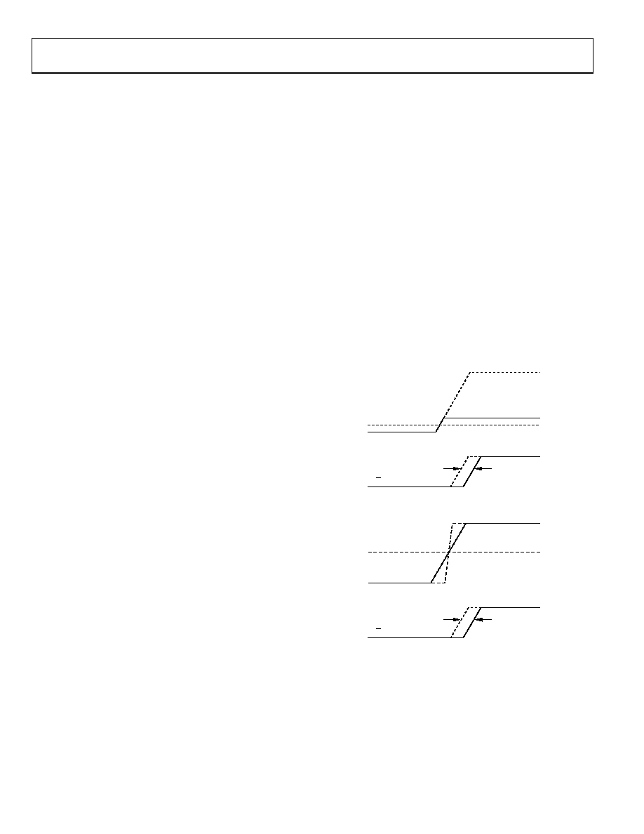
COMPARATOR PROPAGATION DELAY DISPERSION
The ADCMP58x family of comparators has been specifically
designed to reduce propagation delay dispersion over a wide
input overdrive range of 5 mV to 500 mV. Propagation delay
dispersion is a change in propagation delays that results
from a change in the degree of overdrive or slew rate (how far
or fast the input signal exceeds the switching threshold). The
overall result is a higher degree of timing accuracy.
Propagation delay dispersion is a specification that becomes
important in critical timing applications, such as data commu-
nications, automatic test and measurement, instrumentation,
and event-driven applications, such as pulse spectroscopy,
nuclear instrumentation, and medical imaging. Dispersion
is defined as the variation in the overall propagation delay as
the input overdrive conditions are changed (see Figure 26 and
Figure 27). For the ADCMP58x family of comparators, disper-
sion is typically <25 ps, because the overdrive varies from 5 mV
to 500 mV, and the input slew rate varies from 1 V/ns to 10 V/ns.
This specification applies for both positive and negative signals
because the ADCMP58x family of comparators has almost
equal delays for positive- and negative-going inputs.
Q/Q OUTPUT
INPUT VOLTAGE
500mV OVERDRIVE
5mV OVERDRIVE
DISPERSION
VN ± VOS
04
67
2-
0
26
Figure 26. Propagation Delay—Overdrive Dispersion
Q/Q OUTPUT
INPUT VOLTAGE
10V/ns
1V/ns
DISPERSION
VN ± VOS
0
46
72
-02
7
Figure 27. Propagation Delay—Slew Rate Dispersion
相关PDF资料 |
PDF描述 |
|---|---|
| ADCMP572BCPZ-WP | IC COMPARATOR CML 3.3-5V 16LFCSP |
| VE-J4V-MY-F4 | CONVERTER MOD DC/DC 5.8V 50W |
| VI-JNW-MY-F2 | CONVERTER MOD DC/DC 5.5V 50W |
| VE-2WN-MY-B1 | CONVERTER MOD DC/DC 18.5V 50W |
| VE-2N4-CV-B1 | CONVERTER MOD DC/DC 48V 150W |
相关代理商/技术参数 |
参数描述 |
|---|---|
| ADCMP600 | 制造商:Analog Devices 功能描述:- Tape and Reel |
| ADCMP600_11 | 制造商:AD 制造商全称:Analog Devices 功能描述:Rail-to-Rail, Very Fast, 2.5 V to 5.5 V |
| ADCMP600BKSZ-R2 | 功能描述:IC COMP TTL/CMOS 1CHAN SC70-5 RoHS:是 类别:集成电路 (IC) >> 线性 - 比较器 系列:- 产品培训模块:Lead (SnPb) Finish for COTS Obsolescence Mitigation Program 标准包装:2,500 系列:- 类型:通用 元件数:1 输出类型:CMOS,推挽式,满摆幅,TTL 电压 - 电源,单路/双路(±):2.5 V ~ 5.5 V,±1.25 V ~ 2.75 V 电压 - 输入偏移(最小值):5mV @ 5.5V 电流 - 输入偏压(最小值):1pA @ 5.5V 电流 - 输出(标准):- 电流 - 静态(最大值):24µA CMRR, PSRR(标准):80dB CMRR,80dB PSRR 传输延迟(最大):450ns 磁滞:±3mV 工作温度:-40°C ~ 85°C 封装/外壳:6-WFBGA,CSPBGA 安装类型:表面贴装 包装:管件 其它名称:Q3554586 |
| ADCMP600BKSZ-REEL7 | 功能描述:IC COMP TTL/CMOS 1CHAN SC70-5 RoHS:是 类别:集成电路 (IC) >> 线性 - 比较器 系列:- 产品培训模块:Lead (SnPb) Finish for COTS Obsolescence Mitigation Program 标准包装:50 系列:- 类型:带电压基准 元件数:4 输出类型:开路漏极 电压 - 电源,单路/双路(±):2.5 V ~ 11 V,±1.25 V ~ 5.5 V 电压 - 输入偏移(最小值):10mV @ 5V 电流 - 输入偏压(最小值):- 电流 - 输出(标准):0.015mA @ 5V 电流 - 静态(最大值):8.5µA CMRR, PSRR(标准):80dB CMRR,80dB PSRR 传输延迟(最大):- 磁滞:- 工作温度:0°C ~ 70°C 封装/外壳:16-SOIC(0.154",3.90mm 宽) 安装类型:表面贴装 包装:管件 产品目录页面:1386 (CN2011-ZH PDF) |
| ADCMP600BKSZ-RL | 功能描述:IC COMP TTL/CMOS 1CHAN SC70-5 RoHS:是 类别:集成电路 (IC) >> 线性 - 比较器 系列:- 标准包装:25 系列:- 类型:带电压基准 元件数:4 输出类型:CMOS,开路漏极,TTL 电压 - 电源,单路/双路(±):2 V ~ 11 V,±1 V ~ 5.5 V 电压 - 输入偏移(最小值):10mV @ 5V 电流 - 输入偏压(最小值):- 电流 - 输出(标准):0.015mA @ 5V 电流 - 静态(最大值):8.5µA CMRR, PSRR(标准):80dB CMRR,80dB PSRR 传输延迟(最大):12µs 磁滞:50mV 工作温度:0°C ~ 70°C 封装/外壳:16-DIP(0.300",7.62mm) 安装类型:通孔 包装:管件 |
发布紧急采购,3分钟左右您将得到回复。