- 您现在的位置:买卖IC网 > PDF目录2064 > ADCMP601BKSZ-R2 (Analog Devices Inc)IC COMP TTL/CMOS 1CHAN SC70-6 PDF资料下载
参数资料
| 型号: | ADCMP601BKSZ-R2 |
| 厂商: | Analog Devices Inc |
| 文件页数: | 12/16页 |
| 文件大小: | 0K |
| 描述: | IC COMP TTL/CMOS 1CHAN SC70-6 |
| 标准包装: | 250 |
| 类型: | 带锁销 |
| 元件数: | 1 |
| 输出类型: | CMOS,TTL |
| 电压 - 电源,单路/双路(±): | 2.5 V ~ 5.5 V |
| 电压 - 输入偏移(最小值): | 5mV @ 2.5V |
| 电流 - 输入偏压(最小值): | 5µA @ 2.5V |
| 电流 - 输出(标准): | 50mA |
| 电流 - 静态(最大值): | 4mA |
| CMRR, PSRR(标准): | 50dB CMRR,50dB PSRR |
| 传输延迟(最大): | 5ns |
| 磁滞: | 100µV |
| 工作温度: | -40°C ~ 125°C |
| 封装/外壳: | 6-TSSOP,SC-88,SOT-363 |
| 安装类型: | 表面贴装 |
| 包装: | 带卷 (TR) |
ADCMP600/ADCMP601/ADCMP602
Rev. A | Page 5 of 16
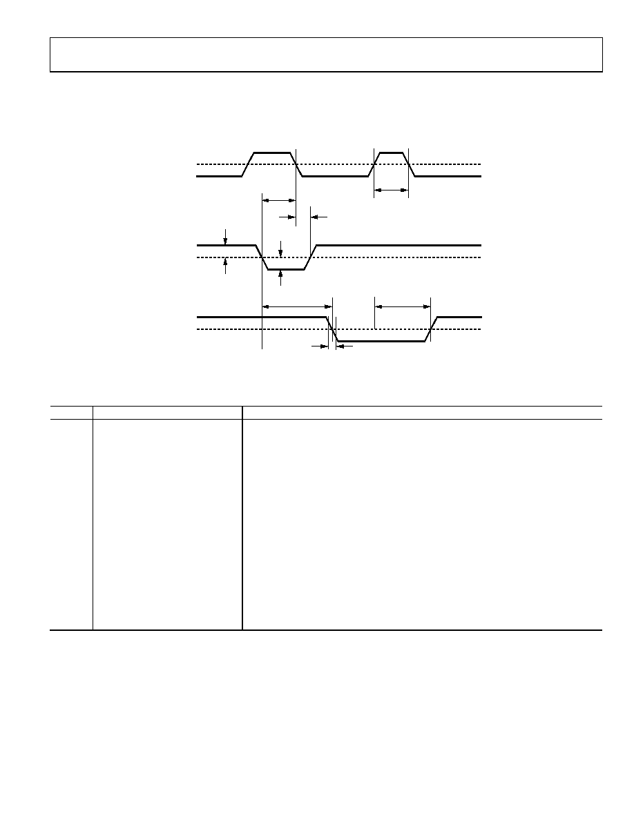
TIMING INFORMATION
Figure 2 illustrates the ADCMP600/ADCMP601/ADCMP602 latch timing relationships. Table 2 provides definitions of the terms shown
1.1V
50%
VN ± VOS
DIFFERENTIAL
INPUT VOLTAGE
LATCH ENABLE
Q OUTPUT
tH
tPDL
tPLOH
tF
VIN
VOD
tS
tPL
05914-
025
Figure 2. System Timing Diagram
Table 2. Timing Descriptions
Symbol
Timing
Description
t
PDH
Input to output high delay
Propagation delay measured from the time the input signal crosses the reference (± the
input offset voltage) to the 50% point of an output low-to-high transition.
t
PDL
Input to output low delay
Propagation delay measured from the time the input signal crosses the reference (± the
input offset voltage) to the 50% point of an output high-to-low transition.
t
PLOH
Latch enable to output high delay
Propagation delay measured from the 50% point of the latch enable signal low-to-high
transition to the 50% point of an output low-to-high transition.
t
PLOL
Latch enable to output low delay
Propagation delay measured from the 50% point of the latch enable signal low-to-high
transition to the 50% point of an output high-to-low transition.
t
H
Minimum hold time
Minimum time after the negative transition of the latch enable signal that the input signal
must remain unchanged to be acquired and held at the outputs.
t
PL
Minimum latch enable pulse width
Minimum time that the latch enable signal must be high to acquire an input signal change.
t
S
Minimum setup time
Minimum time before the negative transition of the latch enable signal occurs that an
input signal change must be present to be acquired and held at the outputs.
t
R
Output rise time
Amount of time required to transition from a low to a high output as measured at the 20%
and 80% points.
t
F
Output fall time
Amount of time required to transition from a high to a low output as measured at the 20%
and 80% points.
V
OD
Voltage overdrive
Difference between the input voltages V
A and VB.
相关PDF资料 |
PDF描述 |
|---|---|
| ADCMP603BCPZ-WP | IC COMP TTL/CMOS 1CHAN 12-LFCSP |
| ADCMP605BCPZ-R2 | IC COMP TTL/CMOS 1CHAN 12-LFCSP |
| ADCMP607BCPZ-R2 | IC COMP TTL/CMOS 1CHAN 12-LFCSP |
| ADCMP608BKSZ-R2 | IC COMP TTL/CMOS R-R SGL SC70-6 |
| ADCMP609BRMZ-REEL | IC COMP TTL/CMOS R-R SGL 8-MSOP |
相关代理商/技术参数 |
参数描述 |
|---|---|
| ADCMP601BKSZ-REEL7 | 功能描述:IC COMP TTL/CMOS 1CHAN SC70-6 RoHS:是 类别:集成电路 (IC) >> 线性 - 比较器 系列:- 标准包装:1 系列:- 类型:通用 元件数:1 输出类型:CMOS,开路集电极,TTL 电压 - 电源,单路/双路(±):2.7 V ~ 5.5 V 电压 - 输入偏移(最小值):7mV @ 5V 电流 - 输入偏压(最小值):0.25µA @ 5V 电流 - 输出(标准):84mA @ 5V 电流 - 静态(最大值):120µA CMRR, PSRR(标准):- 传输延迟(最大):600ns 磁滞:- 工作温度:-40°C ~ 85°C 封装/外壳:SC-74A,SOT-753 安装类型:表面贴装 包装:剪切带 (CT) 产品目录页面:1268 (CN2011-ZH PDF) 其它名称:*LMV331M5*LMV331M5/NOPBLMV331M5CT |
| ADCMP601BKSZ-RL | 功能描述:IC COMP TTL/CMOS 1CHAN SC70-6 RoHS:是 类别:集成电路 (IC) >> 线性 - 比较器 系列:- 标准包装:25 系列:- 类型:带电压基准 元件数:4 输出类型:CMOS,开路漏极,TTL 电压 - 电源,单路/双路(±):2 V ~ 11 V,±1 V ~ 5.5 V 电压 - 输入偏移(最小值):10mV @ 5V 电流 - 输入偏压(最小值):- 电流 - 输出(标准):0.015mA @ 5V 电流 - 静态(最大值):8.5µA CMRR, PSRR(标准):80dB CMRR,80dB PSRR 传输延迟(最大):12µs 磁滞:50mV 工作温度:0°C ~ 70°C 封装/外壳:16-DIP(0.300",7.62mm) 安装类型:通孔 包装:管件 |
| ADCMP602 | 制造商:AD 制造商全称:Analog Devices 功能描述:Rail-to-Rail, Very Fast, 2.5 V to 5.5 V, Single-Supply TTL/CMOS Comparators |
| ADCMP602BRMZ | 功能描述:IC COMP TTL/CMOS 1CHAN 8-MSOP RoHS:是 类别:集成电路 (IC) >> 线性 - 比较器 系列:- 标准包装:1 系列:- 类型:通用 元件数:1 输出类型:CMOS,开路集电极,TTL 电压 - 电源,单路/双路(±):2.7 V ~ 5.5 V 电压 - 输入偏移(最小值):7mV @ 5V 电流 - 输入偏压(最小值):0.25µA @ 5V 电流 - 输出(标准):84mA @ 5V 电流 - 静态(最大值):120µA CMRR, PSRR(标准):- 传输延迟(最大):600ns 磁滞:- 工作温度:-40°C ~ 85°C 封装/外壳:SC-74A,SOT-753 安装类型:表面贴装 包装:剪切带 (CT) 产品目录页面:1268 (CN2011-ZH PDF) 其它名称:*LMV331M5*LMV331M5/NOPBLMV331M5CT |
| ADCMP602BRMZ-REEL | 功能描述:IC COMP TTL/CMOS 1CHAN 8-MSOP RoHS:是 类别:集成电路 (IC) >> 线性 - 比较器 系列:- 标准包装:25 系列:- 类型:带电压基准 元件数:4 输出类型:CMOS,开路漏极,TTL 电压 - 电源,单路/双路(±):2 V ~ 11 V,±1 V ~ 5.5 V 电压 - 输入偏移(最小值):10mV @ 5V 电流 - 输入偏压(最小值):- 电流 - 输出(标准):0.015mA @ 5V 电流 - 静态(最大值):8.5µA CMRR, PSRR(标准):80dB CMRR,80dB PSRR 传输延迟(最大):12µs 磁滞:50mV 工作温度:0°C ~ 70°C 封装/外壳:16-DIP(0.300",7.62mm) 安装类型:通孔 包装:管件 |
发布紧急采购,3分钟左右您将得到回复。