- 您现在的位置:买卖IC网 > PDF目录10688 > ADCMP604BKSZ-RL (Analog Devices Inc)IC COMP TTL/CMOS 1CHAN SC70-6 PDF资料下载
参数资料
| 型号: | ADCMP604BKSZ-RL |
| 厂商: | Analog Devices Inc |
| 文件页数: | 4/16页 |
| 文件大小: | 0K |
| 描述: | IC COMP TTL/CMOS 1CHAN SC70-6 |
| 标准包装: | 10,000 |
| 类型: | 通用 |
| 元件数: | 1 |
| 输出类型: | 补充型,LVDS,满摆幅 |
| 电压 - 电源,单路/双路(±): | 2.5 V ~ 5.5 V |
| 电压 - 输入偏移(最小值): | 5mV @ 3V |
| 电流 - 输入偏压(最小值): | 5µA @ 3V |
| 电流 - 输出(标准): | 50mA |
| 电流 - 静态(最大值): | 21mA |
| CMRR, PSRR(标准): | 50dB CMRR,50dB PSRR |
| 传输延迟(最大): | 3ns |
| 磁滞: | 100µV |
| 工作温度: | -40°C ~ 125°C |
| 封装/外壳: | 6-TSSOP,SC-88,SOT-363 |
| 安装类型: | 表面贴装 |
| 包装: | 带卷 (TR) |
ADCMP604/ADCMP605
Rev. A | Page 12 of 16
The hysteresis control pin appears as a 1.25 V bias voltage
seen through a series resistance of 70 kΩ ± 20% throughout the
hysteresis control range. The advantages of applying hysteresis
in this manner are improved accuracy, improved stability, reduced
component count, and maximum versatility. An external bypass
capacitor is not recommended on the HYS pin because it would
likely degrade the jitter performance of the device and impair the
latch function. As described in the Using/Disabling the Latch
Feature section, hysteresis control need not compromise the
latch function.
0
50
100
150
200
250
50
100
150
200
250
300
350
400
450
500
HYSTERESIS RESISTOR (k)
H
Y
ST
E
R
ES
IS
(
m
V
)
VCC = 2.5V
VCC = 5.5V
05
91
6-
0
26
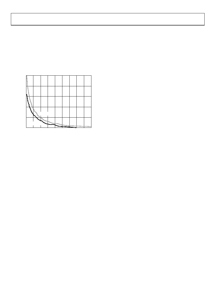
Figure 20. Hysteresis vs. RHYS Control Resistor
CROSSOVER BIAS POINTS
Rail-to-rail inputs of this type, in both op amps and comparators,
have a dual front-end design. Certain devices are active near
the VCCI rail and others are active near the VEE rail. At some pre-
determined point in the common-mode range, a crossover
occurs. At this point, normally VCCI/2, the direction of the bias
current reverses and there are changes in measured offset
voltages and currents.
MINIMUM INPUT SLEW RATE REQUIREMENT
With the rated load capacitance and normal good PCB design
practice, as discussed in the Optimizing Performance section,
these comparators should be stable at any input slew rate with
no hysteresis. Broadband noise from the input stage is observed
in place of the violent chattering seen with most other high
speed comparators. With additional capacitive loading or poor
bypassing, oscillation is observed. This oscillation is due to the
high gain bandwidth of the comparator in combination with
feedback parasitics in the package and PCB. In many applications,
chattering is not harmful.
相关PDF资料 |
PDF描述 |
|---|---|
| ISL83387EIVZ | IC TXRX RS232 ESD 24TSSOP |
| ICL3223ECAZ | IC 2DRVR/2RCVR RS232 3V 20-SSOP |
| ADCMP606BKSZ-REEL7 | IC COMP TTL/CMOS 1CHAN SC70-6 |
| LTC1540IMS8 | IC COMP 300NA 2% VOLT REF 8-MSOP |
| LT1017CSW#TRPBF | IC COMPARATOR MCRPWR DUAL 16SOIC |
相关代理商/技术参数 |
参数描述 |
|---|---|
| ADCMP604BKSZ-RL1 | 制造商:AD 制造商全称:Analog Devices 功能描述:Rail-to-Rail, Very Fast, 2.5 V to 5.5 V, Single-Supply LVDS Comparators |
| ADCMP605 | 制造商:AD 制造商全称:Analog Devices 功能描述:Rail-to-Rail, Very Fast, 2.5 V to 5.5 V, Single-Supply LVDS Comparators |
| ADCMP605BCPZ-R2 | 功能描述:IC COMP TTL/CMOS 1CHAN 12-LFCSP RoHS:是 类别:集成电路 (IC) >> 线性 - 比较器 系列:- 产品培训模块:Lead (SnPb) Finish for COTS Obsolescence Mitigation Program 标准包装:2,500 系列:- 类型:通用 元件数:1 输出类型:CMOS,推挽式,满摆幅,TTL 电压 - 电源,单路/双路(±):2.5 V ~ 5.5 V,±1.25 V ~ 2.75 V 电压 - 输入偏移(最小值):5mV @ 5.5V 电流 - 输入偏压(最小值):1pA @ 5.5V 电流 - 输出(标准):- 电流 - 静态(最大值):24µA CMRR, PSRR(标准):80dB CMRR,80dB PSRR 传输延迟(最大):450ns 磁滞:±3mV 工作温度:-40°C ~ 85°C 封装/外壳:6-WFBGA,CSPBGA 安装类型:表面贴装 包装:管件 其它名称:Q3554586 |
| ADCMP605BCPZ-R21 | 制造商:AD 制造商全称:Analog Devices 功能描述:Rail-to-Rail, Very Fast, 2.5 V to 5.5 V, Single-Supply LVDS Comparators |
| ADCMP605BCPZ-R7 | 功能描述:IC COMP TTL/CMOS 1CHAN 12-LFCSP RoHS:是 类别:集成电路 (IC) >> 线性 - 比较器 系列:- 标准包装:1 系列:- 类型:通用 元件数:1 输出类型:CMOS,开路集电极,TTL 电压 - 电源,单路/双路(±):2.7 V ~ 5.5 V 电压 - 输入偏移(最小值):7mV @ 5V 电流 - 输入偏压(最小值):0.25µA @ 5V 电流 - 输出(标准):84mA @ 5V 电流 - 静态(最大值):120µA CMRR, PSRR(标准):- 传输延迟(最大):600ns 磁滞:- 工作温度:-40°C ~ 85°C 封装/外壳:SC-74A,SOT-753 安装类型:表面贴装 包装:剪切带 (CT) 产品目录页面:1268 (CN2011-ZH PDF) 其它名称:*LMV331M5*LMV331M5/NOPBLMV331M5CT |
发布紧急采购,3分钟左右您将得到回复。