- 您现在的位置:买卖IC网 > PDF目录2064 > ADDI7100BCPZRL (Analog Devices Inc)IC PROCESSOR CCD SIGNAL7 32LFCSP PDF资料下载
参数资料
| 型号: | ADDI7100BCPZRL |
| 厂商: | Analog Devices Inc |
| 文件页数: | 4/20页 |
| 文件大小: | 0K |
| 描述: | IC PROCESSOR CCD SIGNAL7 32LFCSP |
| 标准包装: | 5,000 |
| 类型: | CCD 信号处理器,12 位 |
| 应用: | 数码相机 |
| 安装类型: | 表面贴装 |
| 封装/外壳: | 32-VFQFN 裸露焊盘,CSP |
| 供应商设备封装: | 32-LFCSP-VQ(5x5) |
| 包装: | 带卷 (TR) |
ADDI7100
Rev. C | Page 12 of 20
CIRCUIT DESCRIPTION AND OPERATION
0.1F
07
60
8-
01
0
6dB TO 42dB
CCDIN
CLPOB
DC RESTORE
OPTICAL BLACK
CLAMP
12-BIT
ADC
DAC
11
10
INTERNAL
VREF
2V FULL SCALE
12
CLPOB
PBLK
DATACLK
DATA
OUTPUT
LATCH
SHP
SHD
PBLK
DCBYP
SHP
–3dB, 0dB,
+3dB, +6dB
VGA
CDS
VGA GAIN
REGISTER
DIGITAL
FILTERING
CLAMP LEVEL
REGISTER
BLANK TO
ZERO OR
CLAMP LEVEL
DOUT
D0 TO D11
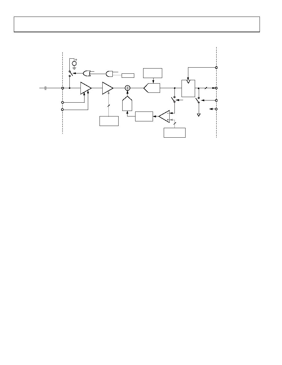
Figure 12. CCD Mode Block Diagram
The ADDI7100 signal processing chain is shown in Figure 12.
Each processing step is essential for achieving a high quality
image from the raw CCD pixel data.
DC RESTORE
To reduce the large dc offset of the CCD output signal, a dc
restore circuit is used with an external 0.1 μF series coupling
capacitor. This circuit restores the dc level of the CCD signal
to approximately 1.5 V, which is compatible with the 3 V supply
of the ADDI7100.
CORRELATED DOUBLE SAMPLER (CDS)
The CDS circuit samples each CCD pixel twice to extract video
information and to reject low frequency noise. The timing
shown in Figure 3 illustrates how the two CDS clocks, SHP and
SHD, are used to sample the reference level and the data level,
respectively, of the CCD signal. The CCD signal is sampled on
the rising edges of SHP and SHD. Placement of these two clock
signals is critical for achieving the best performance from the
CCD. An internal SHP/SHD delay (tID) of 4 ns is caused by
internal propagation delays.
OPTICAL BLACK CLAMP
The optical black clamp loop removes residual offsets in the
signal chain and tracks low frequency variations in the CCD
black level. During the optical black (shielded) pixel interval
on each line, the ADC output is compared with the fixed black
level reference selected by the user in the clamp level register
(Address 0x04). The resulting error signal is filtered to reduce
noise, and the correction value is applied to the ADC input
through a DAC. Normally, the optical black clamp loop is turned
on once per horizontal line, but this loop can be updated more
slowly to suit a particular application. If external digital clamping
is used during postprocessing, optical black clamping for the
ADDI7100 can be disabled using Address 0x00, Bit 2. When the
optical black clamp loop is disabled, the clamp level register can
still be used to provide programmable offset adjustment.
Note that if the CLPOB is disabled, higher VGA gain settings
reduce the dynamic range because the uncorrected offset in the
signal path is amplified.
Horizontal timing is shown in Figure 4. Align the CLPOB pulse
with the optical black pixels of the CCD. It is recommended that
the CLPOB pulse be used during valid CCD dark pixels. It is
recommended that the CLPOB pulse should be 20 pixels wide
to minimize clamp noise. Shorter pulse widths can be used, but
the ability of the loop to track low frequency variations in the
black level is reduced.
相关PDF资料 |
PDF描述 |
|---|---|
| ADDI9023BBCZ | IC DRVR CCD VERT 12CH 40CSPBGA |
| ADG3123BRUZ-REEL7 | IC LEVEL TRANSLATOR 8CH 20-TSSOP |
| ADG3231BRJ-REEL7 | IC SW LLT 1.65/3.6 LV SOT23-6 |
| ADG3232BRJ-REEL7 | IC SW LLT 1.65/3.6 LV SOT23-8 |
| ADG3233BRM-REEL | IC SW LLT 1.65/3.6V BYPASS 8MSOP |
相关代理商/技术参数 |
参数描述 |
|---|---|
| ADDI9000BBCZRL | 制造商:Analog Devices 功能描述: |
| ADDI9000BCBZRL | 制造商:Analog Devices 功能描述:DRIVER |
| ADDI9000XCBZ | |
| ADDI9001BBCZ | 制造商:Analog Devices 功能描述: |
| ADDI9001BBCZRL | 制造商:Analog Devices 功能描述: |
发布紧急采购,3分钟左右您将得到回复。