- 您现在的位置:买卖IC网 > PDF目录20624 > ADE7759ARSRL (Analog Devices Inc)IC ENERGY METERING 1PHASE 20SSOP PDF资料下载
参数资料
| 型号: | ADE7759ARSRL |
| 厂商: | Analog Devices Inc |
| 文件页数: | 7/36页 |
| 文件大小: | 0K |
| 描述: | IC ENERGY METERING 1PHASE 20SSOP |
| 标准包装: | 1,500 |
| 输入阻抗: | 390 千欧 |
| 测量误差: | 0.1% |
| 电压 - 高输入/输出: | 2.4V |
| 电压 - 低输入/输出: | 0.8V |
| 电流 - 电源: | 3mA |
| 电源电压: | 4.75 V ~ 5.25 V |
| 测量仪表类型: | 单相 |
| 工作温度: | -40°C ~ 85°C |
| 安装类型: | 表面贴装 |
| 封装/外壳: | 20-SSOP(0.209",5.30mm 宽) |
| 供应商设备封装: | 20-SSOP |
| 包装: | 带卷 (TR) |
| 配用: | EVAL-ADE7759EBZ-ND - BOARD EVALUATION FOR ADE7759 |
第1页第2页第3页第4页第5页第6页当前第7页第8页第9页第10页第11页第12页第13页第14页第15页第16页第17页第18页第19页第20页第21页第22页第23页第24页第25页第26页第27页第28页第29页第30页第31页第32页第33页第34页第35页第36页
�� ���
���
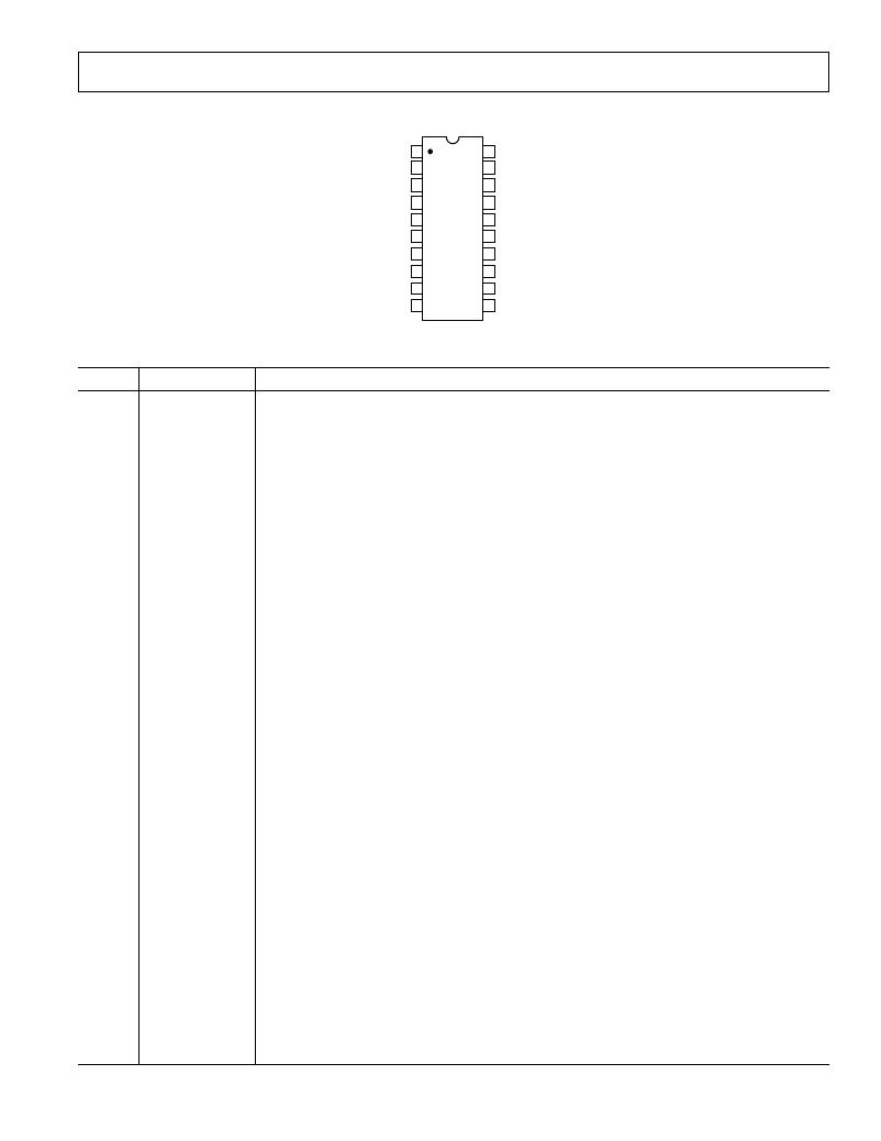
���ADE7759�
�PIN� CONFIGURATION�
�RESET� 1�
�DV� DD� 2�
�AV� DD� 3�
�V1P� 4�
�20�
�19�
�18�
�17�
�DIN�
�DOUT�
�SCLK�
�CS�
�V1N� 5�
�ADE7759�
�16�
�CLKOUT�
�V2N� 6�
�V2P� 7�
�TOP� VIEW�
�(Not� to� Scale)�
�15� CLKIN�
�14� IRQ�
�AGND� 8�
�REF� IN/OUT� 9�
�DGND� 10�
�13�
�12�
�11�
�SAG�
�ZX�
�CF�
�PIN� FUNCTION� DESCRIPTIONS�
�Pin� No.�
�1�
�2�
�3�
�4,� 5�
�6,� 7�
�8�
�9�
�10�
�11�
�REV.� A�
�Mnemonic�
�RESET�
�DV� DD�
�AV� DD�
�V1P,� V1N�
�V2N,� V2P�
�AGND�
�REF� IN/OUT�
�DGND�
�CF�
�Description�
�Reset� Pin� for� the� ADE7759.� A� logic� low� on� this� pin� will� hold� the� ADCs� and� digital� circuitry�
�(including� the� serial� interface)� in� a� reset� condition.�
�Digital� Power� Supply.� This� pin� provides� the� supply� voltage� for� the� digital� circuitry� in� the� ADE7759.�
�The� supply� voltage� should� be� maintained� at� 5� V� ±� 5%� for� specified� operation.� This� pin� should� be�
�decoupled� to� DGND� with� a� 10� m� F� capacitor� in� parallel� with� a� ceramic� 100� nF� capacitor.�
�Analog� Power� Supply.� This� pin� provides� the� supply� voltage� for� the� analog� circuitry� in� the� ADE7759.�
�The� supply� should� be� maintained� at� 5� V� ±� 5%� for� specified� operation.� Every� effort� should� be� made�
�to� minimize� power� supply� ripple� and� noise� at� this� pin� by� the� use� of� proper� decoupling� method.�
�This� pin� should� be� decoupled� to� AGND� with� a� 10� m� F� capacitor� in� parallel� with� a� ceramic� 100� nF�
�capacitor.�
�Analog� Inputs� for� Channel� 1.� This� channel� is� intended� for� use� with� the� di/dt� current� transducers�
�such� as� Rogowski� coil,� or� other� current� sensors� such� as� shunt� or� current� transformer� (CT).� These�
�inputs� are� fully� differential� voltage� inputs� with� maximum� differential� input� signal� levels� of� ±� 0.5� V,�
�±� 0.25� V,� and� ±� 0.125� V,� depending� on� the� full-scale� selection—see� Analog� Inputs� section.�
�Channel� 1� also� has� a� PGA� with� gain� selections� of� 1,� 2,� 4,� 8,� or� 16.� The� maximum� signal� level� at� these�
�pins� with� respect� to� AGND� is� ±� 0.5� V.� Both� inputs� have� internal� ESD� protection� circuitry.� In� addi-�
�tion,� an� overvoltage� of� ±� 6� V� can� be� sustained� on� these� inputs� without� risk� of� permanent� damage.�
�Analog� Inputs� for� Channel� 2.� This� channel� is� intended� for� use� with� the� voltage� transducer.� These� inputs�
�are� fully� differential� voltage� inputs� with� a� maximum� differential� signal� level� of� ±� 0.5� V.� Channel� 2�
�also� has� a� PGA� with� gain� selections� of� 1,� 2,� 4,� 8,� or� 16.� The� maximum� signal� level� at� these� pins�
�with� respect� to� AGND� is� ±� 0.5� V.� Both� inputs� have� internal� ESD� protection� circuitry,� and� an� over-�
�voltage� of� ±� 6� V� can� be� sustained� on� these� inputs� without� risk� of� permanent� damage.�
�This� pin� provides� the� ground� reference� for� the� analog� circuitry� in� the� ADE7759,� i.e.,� ADCs� and�
�reference.� This� pin� should� be� tied� to� the� analog� ground� plane� or� the� quietest� ground� reference� in�
�the� system.� This� quiet� ground� reference� should� be� used� for� all� analog� circuitry,� e.g.,� antialiasing�
�filters,� current� and� voltage� transducers.� To� keep� ground� noise� around� the� ADE7759� to� a� minimum,�
�the� quiet� ground� plane� should� be� connected� to� the� digital� ground� plane� at� only� one� point.� It� is�
�acceptable� to� place� the� entire� device� on� the� analog� ground� plane—see� Application� Information� section.�
�This� pin� provides� access� to� the� on-chip� voltage� reference.� The� on-chip� reference� has� a� nominal�
�value� of� 2.4� V� ±� 8%� and� a� typical� temperature� coefficient� of� 20� ppm/� ∞� C.� An� external� reference�
�source� may� be� connected� at� this� pin.� In� either� case,� this� pin� should� be� decoupled� to� AGND� with�
�a� 1� m� F� capacitor� in� parallel� with� a� 100� nF� capacitor.�
�This� provides� the� ground� reference� for� the� digital� circuitry� in� the� ADE7759,� i.e.,� multiplier,� filters,�
�and� frequency� output� (CF).� Because� the� digital� return� currents� in� the� ADE7759� are� small,� it� is�
�acceptable� to� connect� this� pin� to� the� analog� ground� plane� of� the� system—see� Application� Information�
�section.� However,� high� bus� capacitance� on� the� DOUT� pin� may� result� in� noisy� digital� current� that�
�affects� performance.�
�Calibration� Frequency� Logic� Output.� The� CF� logic� output� gives� Active� Power� information.� This�
�output� is� intended� to� be� used� for� operational� and� calibration� purposes.� The� full-scale� output� fre-�
�quency� can� be� adjusted� by� writing� to� the� APGAIN,� CFNUM,� and� CFDEN� registers—see� Energy�
�to� Frequency� Conversion� section� .�
�–7� –�
�相关PDF资料 |
PDF描述 |
|---|---|
| HCC65DRXH | CONN EDGECARD 130PS DIP .100 SLD |
| ACM43DRUI | CONN EDGECARD 86POS .156 DIP SLD |
| RBB30DHRN | CONN EDGE DUAL .050 EXTEND 60POS |
| 591D687X06R3R2T20H | CAP TANT 680UF 6.3V 20% 2824 |
| ACC43DRXN | CONN EDGECARD 86POS .100 DIP SLD |
相关代理商/技术参数 |
参数描述 |
|---|---|
| ADE7759ARSZ | 功能描述:IC ENERGY METERING 1PHASE 20SSOP RoHS:是 类别:集成电路 (IC) >> PMIC - 能量测量 系列:- 产品培训模块:Lead (SnPb) Finish for COTS Obsolescence Mitigation Program 标准包装:2,500 系列:* |
| ADE7759ARSZRL | 功能描述:IC ENERGY METERING 1PHASE 20SSOP RoHS:是 类别:集成电路 (IC) >> PMIC - 能量测量 系列:- 产品培训模块:Lead (SnPb) Finish for COTS Obsolescence Mitigation Program 标准包装:2,500 系列:* |
| ADE7760 | 制造商:AD 制造商全称:Analog Devices 功能描述:Energy Metering IC with On-Chip Fault Detection |
| ADE7760ARS | 制造商:Analog Devices 功能描述:Energy Measurement 20-Pin SSOP 制造商:Analog Devices 功能描述:ENERGY METER IC W/ ONCHIP FAULT & OSCIL. - Rail/Tube |
| ADE7760ARSRL | 制造商:Analog Devices 功能描述:Energy Measurement 20-Pin SSOP T/R 制造商:Analog Devices 功能描述:ENERGY METER IC W/ONCHIP FAULT & OSCIL. - Tape and Reel |
发布紧急采购,3分钟左右您将得到回复。