- 您现在的位置:买卖IC网 > PDF目录9112 > ADF4001BRUZ-R7 (Analog Devices Inc)IC CLOCK GEN PLL 200MHZ 16TSSOP PDF资料下载
参数资料
| 型号: | ADF4001BRUZ-R7 |
| 厂商: | Analog Devices Inc |
| 文件页数: | 6/17页 |
| 文件大小: | 0K |
| 描述: | IC CLOCK GEN PLL 200MHZ 16TSSOP |
| 标准包装: | 1,000 |
| 类型: | 时钟发生器(RF) |
| PLL: | 是 |
| 输入: | 时钟 |
| 输出: | 时钟 |
| 电路数: | 1 |
| 比率 - 输入:输出: | 2:1 |
| 差分 - 输入:输出: | 是/无 |
| 频率 - 最大: | 200MHz |
| 除法器/乘法器: | 是/无 |
| 电源电压: | 2.7 V ~ 5.5 V |
| 工作温度: | -40°C ~ 85°C |
| 安装类型: | 表面贴装 |
| 封装/外壳: | 16-TSSOP(0.173",4.40mm 宽) |
| 供应商设备封装: | 16-TSSOP |
| 包装: | 带卷 (TR) |
REV.
ADF4001
–14–
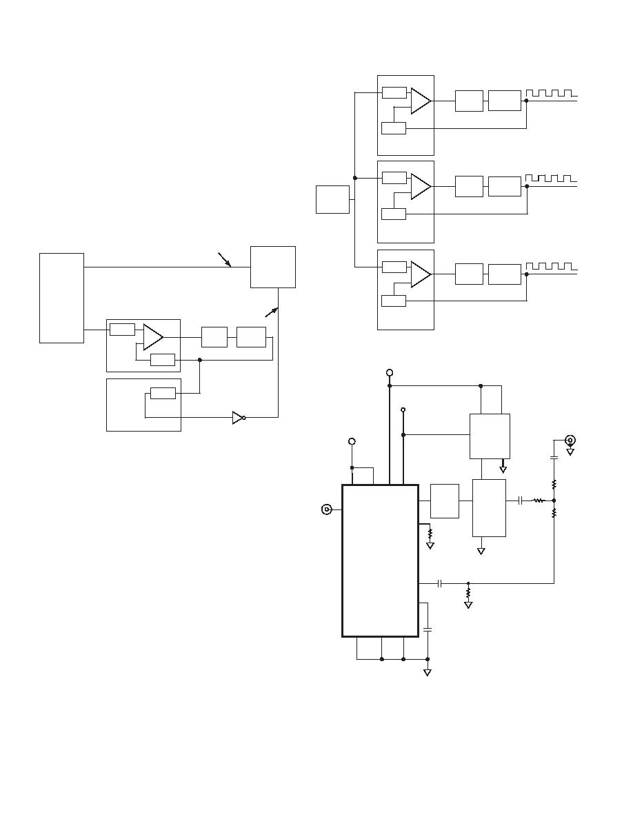
COHERENT CLOCK GENERATION
When testing A/D converters, it is often advantageous to use a
coherent test system, that is, a system that ensures a specific
relationship between the A/D converter input signal and the
A/D converter sample rate. Thus, when doing an FFT on this
data, there is no longer any need to apply the window weighting
function. Figure 8 shows how the ADF4001 can be used to handle
all the possible combinations of the input signal frequency and
sampling rate. The first ADF4001 is phase locked to a VCO. The
output of the VCO is also fed into the N divider of the second
ADF4001. This results in both ADF4001s being coherent with
the REFIN. Since the REFIN comes from the signal generator, the
MUXOUT signal of the second ADF4001 is coherent with the fIN
frequency to the ADC. This is used as fS, the sampling clock.
CPRF
REFIN
f
S
= (f
IN
N1)/(R1
N2)
A/D
CONVERTER
UNDER
TEST
ADF4001
SINE
OUTPUT
BRUEL &
KJAER
MODEL 1051
SQUARE
OUTPUT
VCO
100MHz
LOOP
FILTER
RFIN
MUXOUT
NC7S04
N2
N1
R1
fIN
fS
SAMPLING
CLOCK
AIN
Figure 8. Coherent Clock Generator
TRI-BAND CLOCK GENERATION CIRCUIT
In multiband applications, it is necessary to realize different
clocks from one master clock frequency. For example, GSM
uses a 13 MHz system clock, WCDMA uses 19.44 MHz, and
CDMA uses 19.2 MHz. The circuit in Figure 9 shows how to
use the ADF4001 to generate GSM, WCDMA, and CDMA
system clocks from a single 52 MHz master clock. The low RF
fMIN specification and the ability to program R and N values as
low as
1 makes the ADF4001 suitable for this. Other fOUT
clock frequencies can be realized using the formula
f
REF
N
R
OUT
IN
=×
÷
()
SHUTDOWN CIRCUIT
The circuit in Figure 10 shows how to shut down both the
ADF4001 and the accompanying VCO. The ADG702 switch
goes open circuit when a Logic 1 is applied to the IN input.
The low cost switch is available in both SOT-23 and micro
SOIC packages.
19.44MHz SYSTEM
CLOCK FOR WCDMA
19.2MHz SYSTEM
CLOCK FOR CDMA
13MHz SYSTEM
CLOCK FOR GSM
R2
1300
ADF4001
RFIN
REFIN
CPRF
65
R3
CPRF
ADF4001
REFIN
RFIN
R1
4
REFIN
RFIN
ADF4001
CPRF
52MHz
MASTER
CLOCK
N2
486
LOOP
FILTER
VCXO
19.44MHz
N1
1
N3
24
VCXO
13MHz
VCXO
19.2MHz
LOOP
FILTER
LOOP
FILTER
Figure 9. Tri-Band System Clock Generation
FREFIN
AGND
4
DGND
9
CPGND
3
ADF4001
RFINA
RFINB
100pF
51
AVDD
VDD
7
DVDD
15
VP
16
CE
10
1
2
RSET
CP
POWER-DOWN CONTROL
DECOUPLING CAPACITORS AND INTERFACE
SIGNALS HAVE BEEN OMITTED FROM THE
DIAGRAM IN THE INTEREST OF GREATER CLARITY.
6
5
10k
LOOP
FILTER
RFOUT
100pF
18
100pF
ADG702
S
D
GND
VDD
IN
VCC
GND
VCO
OR
VCXO
Figure 10. Local Oscillator Shutdown Circuit
B
相关PDF资料 |
PDF描述 |
|---|---|
| VI-21K-MW-S | CONVERTER MOD DC/DC 40V 100W |
| VE-25T-IV | CONVERTER MOD DC/DC 6.5V 150W |
| ADF4001BCPZ-RL | IC CLOCK GEN PLL 200MHZ 20LFCSP |
| VE-B1K-MV-S | CONVERTER MOD DC/DC 40V 150W |
| ADF4001BRUZ-RL | IC CLOCK GEN PLL 200MHZ 16TSSOP |
相关代理商/技术参数 |
参数描述 |
|---|---|
| ADF4001BRUZ-RL | 功能描述:IC CLOCK GEN PLL 200MHZ 16TSSOP RoHS:是 类别:集成电路 (IC) >> 时钟/计时 - 时钟发生器,PLL,频率合成器 系列:- 标准包装:1,000 系列:Precision Edge® 类型:时钟/频率合成器 PLL:无 输入:CML,PECL 输出:CML 电路数:1 比率 - 输入:输出:2:1 差分 - 输入:输出:是/是 频率 - 最大:10.7GHz 除法器/乘法器:无/无 电源电压:2.375 V ~ 3.6 V 工作温度:-40°C ~ 85°C 安装类型:表面贴装 封装/外壳:16-VFQFN 裸露焊盘,16-MLF? 供应商设备封装:16-MLF?(3x3) 包装:带卷 (TR) 其它名称:SY58052UMGTRSY58052UMGTR-ND |
| ADF4001SP1BRU | 制造商:Analog Devices 功能描述:- Rail/Tube |
| ADF4001SP1BRU-RL7 | 制造商:Analog Devices 功能描述: |
| ADF4001SP1BRUZ | 制造商:Analog Devices 功能描述: |
| ADF4001SP1BRUZ-RL7 | 制造商:Analog Devices 功能描述: |
发布紧急采购,3分钟左右您将得到回复。