- 您现在的位置:买卖IC网 > PDF目录9112 > ADF4001BRUZ-R7 (Analog Devices Inc)IC CLOCK GEN PLL 200MHZ 16TSSOP PDF资料下载
参数资料
| 型号: | ADF4001BRUZ-R7 |
| 厂商: | Analog Devices Inc |
| 文件页数: | 7/17页 |
| 文件大小: | 0K |
| 描述: | IC CLOCK GEN PLL 200MHZ 16TSSOP |
| 标准包装: | 1,000 |
| 类型: | 时钟发生器(RF) |
| PLL: | 是 |
| 输入: | 时钟 |
| 输出: | 时钟 |
| 电路数: | 1 |
| 比率 - 输入:输出: | 2:1 |
| 差分 - 输入:输出: | 是/无 |
| 频率 - 最大: | 200MHz |
| 除法器/乘法器: | 是/无 |
| 电源电压: | 2.7 V ~ 5.5 V |
| 工作温度: | -40°C ~ 85°C |
| 安装类型: | 表面贴装 |
| 封装/外壳: | 16-TSSOP(0.173",4.40mm 宽) |
| 供应商设备封装: | 16-TSSOP |
| 包装: | 带卷 (TR) |
REV.
ADF4001
–15–
INTERFACING
The ADF4001 family has a simple SPI
compatible serial inter-
face for writing to the device. SCLK, SDATA, and LE control
the data transfer. When LE (latch enable) goes high, the 24 bits
that have been clocked into the input register on each rising
edge of SCLK will be transferred to the appropriate latch. See
Figure 1 for the Timing Diagram and Table I for the Latch
Truth Table.
The maximum allowable serial clock rate is 20 MHz. This means
that the maximum update rate possible for the device is 833 kHz
or one update every 1.2 ms. This is certainly more than adequate
for systems with typical lock times in hundreds of microseconds.
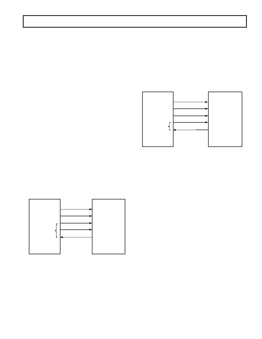
ADuC812 Interface
Figure 11 shows the interface between the ADF4001 family and
the ADuC812 MicroConverter
. Since the ADuC812 is based
on an 8051 core, this interface can be used with any 8051-based
microcontroller. The MicroConverter is set up for SPI master
mode with CPHA = 0. To initiate the operation, the I/O port
driving LE is brought low. Each latch of the ADF4001 family
needs a 24-bit word. This is accomplished by writing three 8-bit
bytes from the MicroConverter to the device. When the third
byte has been written, the LE input should be brought high to
complete the transfer.
On first applying power to the ADF4001 family, it needs three
writes (one each to the R counter latch, the N counter latch, and
the initialization latch) for the output to become active.
I/O port lines on the ADuC812 are also used to control power-
down (CE input) and to detect lock (MUXOUT configured as
lock detect and polled by the port input).
When operating in the mode described, the maximum SCLOCK
rate of the ADuC812 is 4 MHz. This means that the maxi-
mum rate at which the output frequency can be changed will
be 166 kHz.
ADuC812
ADF4001
SCLK
SDATA
LE
CE
MUXOUT
(LOCK DETECT)
SCLOCK
MOSI
I/O PORTS
Figure 11. ADuC812 to ADF4001 Family Interface
ADSP-2181 Interface
Figure 12 shows the interface between the ADF4001 family and
the ADSP-21xx digital signal processor. The ADF4001 family
needs a 24-bit serial word for each latch write. The easiest way
to accomplish this using the ADSP-21xx family is to use the
autobuffered transmit mode of operation with alternate framing.
This provides a means for transmitting an entire block of serial
data before an interrupt is generated. Set up the word length for
8 bits and use three memory locations for each 24-bit word. To
program each 24-bit latch, store the three 8-bit bytes, enable the
autobuffered mode, and then write to the transmit register of
the DSP. This last operation initiates the autobuffer transfer.
ADF4001
SCLK
SDATA
LE
CE
MUXOUT
(LOCK DETECT)
ADSP-21xx
SCLK
I/O FLAGS
DT
TFS
Figure 12. ADSP-21xx to ADF4001 Family Interface
PCB DESIGN GUIDELINES FOR CHIP SCALE PACKAGE
The leads on the chip package (CP-20) are rectangular. The
printed circuit board pad for these should be 0.1 mm longer
than the package lead length and 0.05 mm wider than the
package lead width. The lead should be centered on the pad to
ensure that the solder joint size is maximized.
The bottom of the chip scale package has a central thermal pad.
The thermal pad on the printed circuit board should be at least
as large as this exposed pad. On the printed circuit board, there
should be a clearance of at least 0.25 mm between the thermal
pad and the inner edge of the pad pattern. This will ensure that
shorting is avoided.
Thermal vias may be used on the printed circuit board thermal
pad to improve thermal performance of the package. If vias are
used, they should be incorporated in the thermal pad at 1.2 mm
pitch grid. The via diameter should be between 0.3 mm and
0.33 mm, and the via barrel should be plated with 1 oz. copper
to plug the via.
The user should connect the printed circuit board thermal pad
to AGND.
B
相关PDF资料 |
PDF描述 |
|---|---|
| VI-21K-MW-S | CONVERTER MOD DC/DC 40V 100W |
| VE-25T-IV | CONVERTER MOD DC/DC 6.5V 150W |
| ADF4001BCPZ-RL | IC CLOCK GEN PLL 200MHZ 20LFCSP |
| VE-B1K-MV-S | CONVERTER MOD DC/DC 40V 150W |
| ADF4001BRUZ-RL | IC CLOCK GEN PLL 200MHZ 16TSSOP |
相关代理商/技术参数 |
参数描述 |
|---|---|
| ADF4001BRUZ-RL | 功能描述:IC CLOCK GEN PLL 200MHZ 16TSSOP RoHS:是 类别:集成电路 (IC) >> 时钟/计时 - 时钟发生器,PLL,频率合成器 系列:- 标准包装:1,000 系列:Precision Edge® 类型:时钟/频率合成器 PLL:无 输入:CML,PECL 输出:CML 电路数:1 比率 - 输入:输出:2:1 差分 - 输入:输出:是/是 频率 - 最大:10.7GHz 除法器/乘法器:无/无 电源电压:2.375 V ~ 3.6 V 工作温度:-40°C ~ 85°C 安装类型:表面贴装 封装/外壳:16-VFQFN 裸露焊盘,16-MLF? 供应商设备封装:16-MLF?(3x3) 包装:带卷 (TR) 其它名称:SY58052UMGTRSY58052UMGTR-ND |
| ADF4001SP1BRU | 制造商:Analog Devices 功能描述:- Rail/Tube |
| ADF4001SP1BRU-RL7 | 制造商:Analog Devices 功能描述: |
| ADF4001SP1BRUZ | 制造商:Analog Devices 功能描述: |
| ADF4001SP1BRUZ-RL7 | 制造商:Analog Devices 功能描述: |
发布紧急采购,3分钟左右您将得到回复。