- 您现在的位置:买卖IC网 > PDF目录1989 > ADF4150HVBCPZ (Analog Devices Inc)IC FRACTION-N FREQ SYNTH 32LFCSP PDF资料下载
参数资料
| 型号: | ADF4150HVBCPZ |
| 厂商: | Analog Devices Inc |
| 文件页数: | 13/28页 |
| 文件大小: | 0K |
| 描述: | IC FRACTION-N FREQ SYNTH 32LFCSP |
| 标准包装: | 1 |
| 类型: | * |
| PLL: | 是 |
| 输入: | CMOS |
| 输出: | 时钟 |
| 电路数: | 1 |
| 比率 - 输入:输出: | 1:2 |
| 差分 - 输入:输出: | 无/是 |
| 频率 - 最大: | 3GHz |
| 除法器/乘法器: | 是/无 |
| 电源电压: | 3 V ~ 3.6 V |
| 工作温度: | -40°C ~ 85°C |
| 安装类型: | 表面贴装 |
| 封装/外壳: | 32-WFQFN 裸露焊盘,CSP |
| 供应商设备封装: | 32-LFCSP-WQ(5x5) |
| 包装: | 托盘 |
第1页第2页第3页第4页第5页第6页第7页第8页第9页第10页第11页第12页当前第13页第14页第15页第16页第17页第18页第19页第20页第21页第22页第23页第24页第25页第26页第27页第28页
ADF4150HV
Rev. 0 | Page 20 of 28
RF SYNTHESIZER—A WORKED EXAMPLE
The following equations are used to program the ADF4150HV
synthesizer:
RFOUT = [INT + (FRAC/MOD)] × (fPFD/RF Divider)
(3)
where:
RFOUT is the RF frequency output.
INT is the integer division factor.
FRAC is the fractionality.
MOD is the modulus.
RF Divider is the output divider that divides down the VCO
frequency.
fPFD = REFIN × [(1 + D)/(R × (1 + T))]
(4)
where:
REFIN is the reference frequency input.
D is the RF REFIN doubler bit (0 or 1).
R is the RF reference division factor (1 to 1023).
T is the reference divide-by-2 bit (0 or 1).
In this example, the user wants to program a 1.5 GHz RF
frequency output (RFOUT) with a 500 kHz channel resolution
(fRESOUT) required on the RF output. The reference frequency
input (REFIN) is 25 MHz. The VCO options available to the
user include the following:
1.5 GHz VCO in fundamental mode
3 GHz VCO with the RF divider set to 2
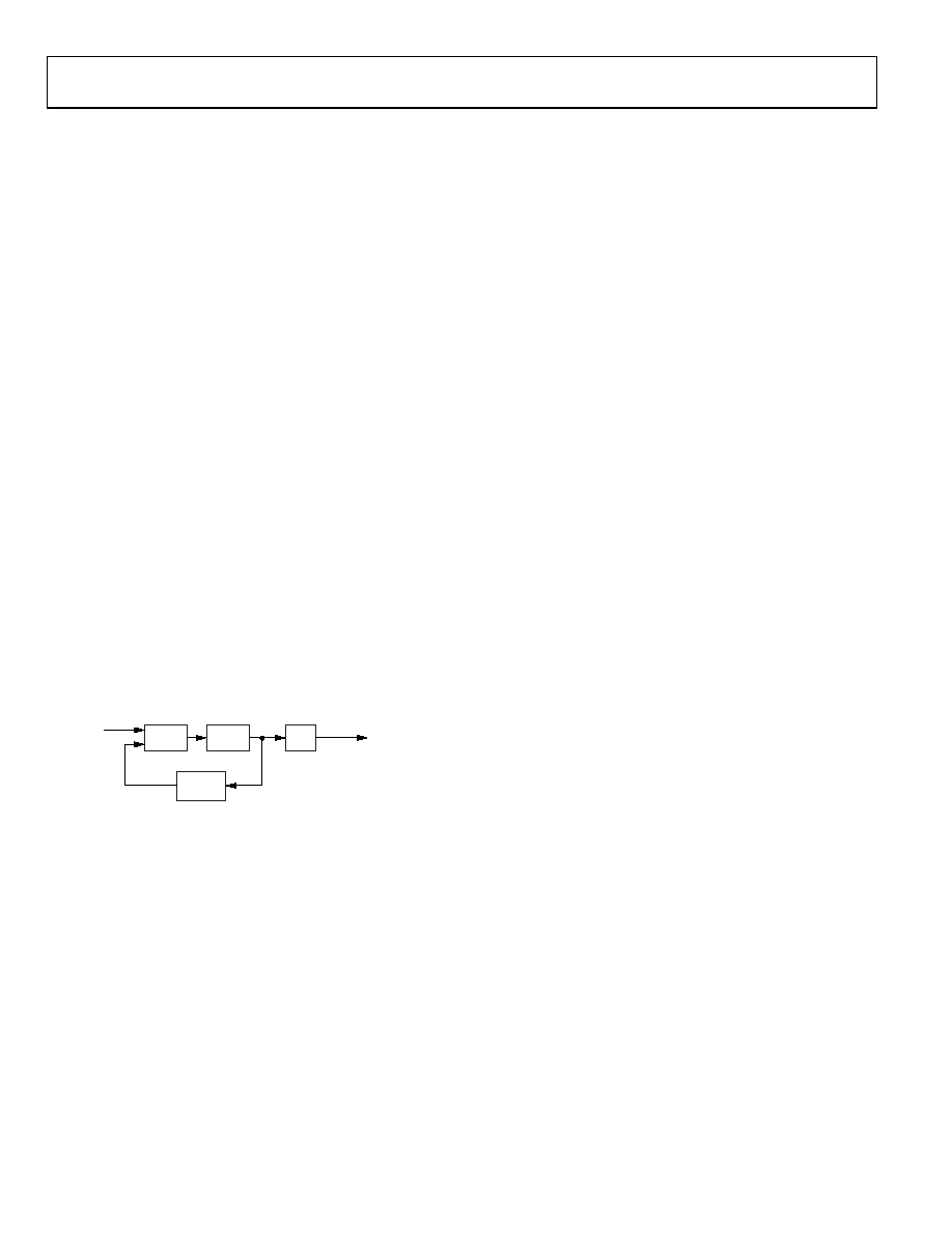
When enabling the RF divider, the user must decide whether to
close the PLL loop before the RF divider or after it. In this
example, the PLL loop is closed before the RF divider (see
fPFD
PFD
VCO
N
DIVIDER
÷2
RFOUT
09
05
8-
02
2
Figure 26. PLL Loop Closed Before Output Divider
To minimize VCO feedthrough, the 3 GHz VCO is selected. A
channel resolution (fRESOUT) of 500 kHz is required at the output
of the RF divider. Therefore, the channel resolution at the output
of the VCO (fRES) needs to be 2 × fRESOUT, that is, 1 MHz.
MOD = REFIN/fRES
MOD = 25 MHz/1 MHz = 25
From Equation 4,
fPFD = [25 MHz × (1 + 0)/1] = 25 MHz
(5)
1500.5 MHz = 25 MHz × [(INT + (FRAC/25))/2]
(6)
where:
INT = 120.
FRAC = 1.
RF Divider = 2.
The ADF4150HV evaluation software can be used to help
determine integer and fractional values for a given setup,
along with the actual register settings to be programmed.
REFERENCE DOUBLER AND REFERENCE DIVIDER
The on-chip reference doubler allows the input reference signal
to be doubled. Doubling the reference signal doubles the PFD
comparison frequency, which improves the noise performance
of the system. Doubling the PFD frequency usually improves
noise performance by 3 dB. Note that the PFD cannot operate
above 32 MHz due to a limitation in the speed of the Σ-Δ circuit
of the N divider.
The reference divide-by-2 divides the reference signal by 2,
resulting in a 50% duty cycle PFD frequency. This is necessary
for the correct operation of the charge pump boost mode. For
more information, see the Boost Enable section.
12-BIT PROGRAMMABLE MODULUS
The choice of modulus (MOD) depends on the reference signal
(REFIN) available and the channel resolution (fRES) required at the
RF output. For example, a GSM system with 13 MHz REFIN sets
the modulus to 65. This means that the RF output resolution
(fRES) is the 200 kHz (13 MHz/65) necessary for GSM. With
dither off, the fractional spur interval depends on the modulus
values chosen (see Table 8).
Unlike most other fractional-N PLLs, the ADF4150HV allows
the user to program the modulus over a 12-bit range. When
combined with the reference doubler and the 10-bit R counter,
the 12-bit modulus allows the user to set up the part in many
different configurations for the application.
For example, consider an application that requires a 1.75 GHz
RF frequency output with a 200 kHz channel step resolution.
The system has a 13 MHz reference signal.
One possible setup is to feed the 13 MHz reference signal
directly into the PFD and to program the modulus to divide
by 65. This setup results in the required 200 kHz resolution.
Another possible setup is to use the reference doubler to create
26 MHz from the 13 MHz input signal. The 26 MHz is then fed
into the PFD, and the modulus is programmed to divide by 130.
This setup also results in 200 kHz resolution but offers superior
phase noise performance over the first setup.
The programmable modulus is also very useful for multistandard
applications with different channel spacing requirements.
It is important that the PFD frequency remain constant (in this
example, 13 MHz). This allows the user to design one loop filter
for both setups without encountering stability issues. Note that
the ratio of the RF frequency to the PFD frequency principally
affects the loop filter design, not the actual channel spacing.
相关PDF资料 |
PDF描述 |
|---|---|
| ADF4151BCPZ-RL7 | IC FRACTION-N FREQ SYNTH 32LFCSP |
| ADF4153YRUZ | IC SYNTH PLL RF F-N FREQ 16TSSOP |
| ADF4154BRU | IC FRAC-N FREQ SYNTH 16-TSSOP |
| ADF4156BRUZ-RL7 | IC PLL FRAC-N FREQ SYNTH 16TSSOP |
| ADF4157BRUZ-RL7 | IC PLL FREQ SYNTH 6GHZ 16TSSOP |
相关代理商/技术参数 |
参数描述 |
|---|---|
| ADF4150HVBCPZ-RL7 | 功能描述:IC FRACTION-N FREQ SYNTH 32LFCSP RoHS:是 类别:集成电路 (IC) >> 时钟/计时 - 时钟发生器,PLL,频率合成器 系列:- 标准包装:1,000 系列:Precision Edge® 类型:时钟/频率合成器 PLL:无 输入:CML,PECL 输出:CML 电路数:1 比率 - 输入:输出:2:1 差分 - 输入:输出:是/是 频率 - 最大:10.7GHz 除法器/乘法器:无/无 电源电压:2.375 V ~ 3.6 V 工作温度:-40°C ~ 85°C 安装类型:表面贴装 封装/外壳:16-VFQFN 裸露焊盘,16-MLF? 供应商设备封装:16-MLF?(3x3) 包装:带卷 (TR) 其它名称:SY58052UMGTRSY58052UMGTR-ND |
| ADF4151 | 制造商:AD 制造商全称:Analog Devices 功能描述:Fractional-N/Integer-N PLL Synthesizer |
| ADF4151BCPZ | 功能描述:IC PLL FREQ SYNTHESIZER 32LFCSP RoHS:是 类别:集成电路 (IC) >> 时钟/计时 - 时钟发生器,PLL,频率合成器 系列:- 标准包装:1,000 系列:Precision Edge® 类型:时钟/频率合成器 PLL:无 输入:CML,PECL 输出:CML 电路数:1 比率 - 输入:输出:2:1 差分 - 输入:输出:是/是 频率 - 最大:10.7GHz 除法器/乘法器:无/无 电源电压:2.375 V ~ 3.6 V 工作温度:-40°C ~ 85°C 安装类型:表面贴装 封装/外壳:16-VFQFN 裸露焊盘,16-MLF? 供应商设备封装:16-MLF?(3x3) 包装:带卷 (TR) 其它名称:SY58052UMGTRSY58052UMGTR-ND |
| ADF4151BCPZ-RL7 | 功能描述:IC FRACTION-N FREQ SYNTH 32LFCSP RoHS:是 类别:集成电路 (IC) >> 时钟/计时 - 时钟发生器,PLL,频率合成器 系列:- 标准包装:1,000 系列:Precision Edge® 类型:时钟/频率合成器 PLL:无 输入:CML,PECL 输出:CML 电路数:1 比率 - 输入:输出:2:1 差分 - 输入:输出:是/是 频率 - 最大:10.7GHz 除法器/乘法器:无/无 电源电压:2.375 V ~ 3.6 V 工作温度:-40°C ~ 85°C 安装类型:表面贴装 封装/外壳:16-VFQFN 裸露焊盘,16-MLF? 供应商设备封装:16-MLF?(3x3) 包装:带卷 (TR) 其它名称:SY58052UMGTRSY58052UMGTR-ND |
| ADF4152HVBCPZ | 功能描述:IC FRACTION-N FREQ SYNTH 32LFCSP 制造商:analog devices inc. 系列:- 包装:托盘 零件状态:在售 类型:* PLL:是 输入:CMOS 输出:时钟 电路数:1 比率 - 输入:输出:2:2 差分 - 输入:输出:是/无 频率 - 最大值:5GHz 分频器/倍频器:是/是 电压 - 电源:3 V ~ 3.6 V 工作温度:-40°C ~ 85°C 安装类型:表面贴装 封装/外壳:32-VFQFN 裸露焊盘,CSP 供应商器件封装:32-LFCSP-VQ(5x5) 标准包装:1 |
发布紧急采购,3分钟左右您将得到回复。