- 您现在的位置:买卖IC网 > PDF目录1989 > ADF4150HVBCPZ (Analog Devices Inc)IC FRACTION-N FREQ SYNTH 32LFCSP PDF资料下载
参数资料
| 型号: | ADF4150HVBCPZ |
| 厂商: | Analog Devices Inc |
| 文件页数: | 18/28页 |
| 文件大小: | 0K |
| 描述: | IC FRACTION-N FREQ SYNTH 32LFCSP |
| 标准包装: | 1 |
| 类型: | * |
| PLL: | 是 |
| 输入: | CMOS |
| 输出: | 时钟 |
| 电路数: | 1 |
| 比率 - 输入:输出: | 1:2 |
| 差分 - 输入:输出: | 无/是 |
| 频率 - 最大: | 3GHz |
| 除法器/乘法器: | 是/无 |
| 电源电压: | 3 V ~ 3.6 V |
| 工作温度: | -40°C ~ 85°C |
| 安装类型: | 表面贴装 |
| 封装/外壳: | 32-WFQFN 裸露焊盘,CSP |
| 供应商设备封装: | 32-LFCSP-WQ(5x5) |
| 包装: | 托盘 |
第1页第2页第3页第4页第5页第6页第7页第8页第9页第10页第11页第12页第13页第14页第15页第16页第17页当前第18页第19页第20页第21页第22页第23页第24页第25页第26页第27页第28页
ADF4150HV
Rev. 0 | Page 25 of 28
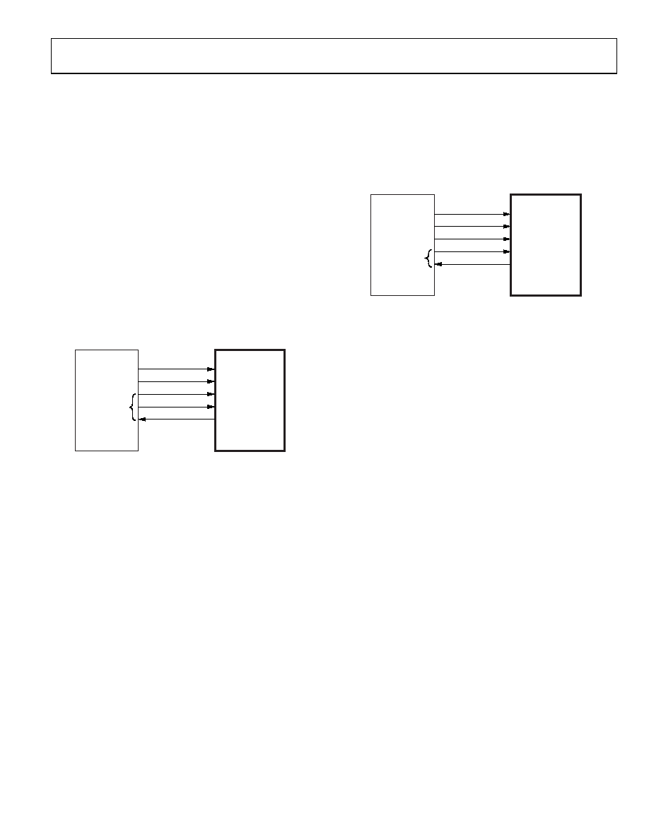
INTERFACING TO THE ADuC702x AND
THE ADSP-BF527
The ADF4150HV has a simple SPI-compatible serial interface for
writing to the device. The CLK, DATA, and LE pins control the
data transfer. When LE goes high, the 32 bits that were clocked
into the appropriate register on each rising edge of CLK are
transferred to the appropriate latch. See Figure 2 for the timing
diagram and Table 6 for the register address table.
ADuC702x Interface
family is based on an ARM7 core, but the same interface can be
used with any 8051-based microcontroller.
The microcontroller is set up for SPI master mode with CPHA =
0. To initiate the operation, the I/O port driving LE is brought
low. Each latch of the ADF4150HV needs a 32-bit word, which
is accomplished by writing four 8-bit bytes from the micro-
controller to the device. After the fourth byte is written, the
LE input should be brought high to complete the transfer.
ADuC702x
ADF4150HV
CLK
DATA
LE
CE
MUXOUT
(LOCK DETECT)
SCLOCK
MOSI
I/O PORTS
09
05
8-
03
0
I/O port lines on the ADuC702x are also used to control the
power-down input (CE) and the lock detect (MUXOUT con-
figured for lock detect and polled by the port input). When
operating in the mode described, the maximum SPI transfer
rate of the ADuC7023 is 20 Mbps. This means that the maxi-
mum rate at which the output frequency can be changed is
833 kHz. If using a faster SPI clock, make sure that the SPI
timing requirements listed in Table 2 are adhered to.
Blackfin ADSP-BF527 Interface
the Blackfin ADSP-BF527 digital signal processor (DSP). The
ADF4150HV needs a 32-bit serial word for each latch write.
The easiest way to accomplish this using the Blackfin family
is to use the autobuffered transmit mode of operation with
alternate framing. This mode provides a means for transmitting
an entire block of serial data before an interrupt is generated.
ADSP-BF527
ADF4150HV
CLK
DATA
LE
CE
MUXOUT
(LOCK DETECT)
SCK
MOSI
GPIO
I/O PORTS
09
05
8-
03
1
Figure 32. ADSP-BF527 to ADF4150HV Interface
Set up the word length for eight bits and use four memory loca-
tions for each 32-bit word. To program each 32-bit latch, store
the 8-bit bytes, enable the autobuffered mode, and write to the
transmit register of the DSP. This last operation initiates the
autobuffer transfer. If using a faster SPI clock, make sure that
the SPI timing requirements listed in Table 2 are adhered to.
PCB DESIGN GUIDELINES FOR A CHIP SCALE
PACKAGE
The lands on the chip scale package (CP-32-11) are rectangular.
The PCB pad for these lands must be 0.1 mm longer than the
package land length and 0.05 mm wider than the package land
width. Each land must be centered on the pad to ensure that the
solder joint size is maximized.
The bottom of the chip scale package has a central exposed
thermal pad. The thermal pad on the PCB must be at least as
large as the exposed pad. On the PCB, there must be a minimum
clearance of 0.25 mm between the thermal pad and the inner
edges of the pad pattern to ensure that shorting is avoided.
Thermal vias can be used on the PCB thermal pad to improve
the thermal performance of the package. If vias are used, they
must be incorporated into the thermal pad at 1.2 mm pitch grid.
The via diameter must be between 0.3 mm and 0.33 mm, and
the via barrel must be plated with 1 oz. of copper to plug the via.
相关PDF资料 |
PDF描述 |
|---|---|
| ADF4151BCPZ-RL7 | IC FRACTION-N FREQ SYNTH 32LFCSP |
| ADF4153YRUZ | IC SYNTH PLL RF F-N FREQ 16TSSOP |
| ADF4154BRU | IC FRAC-N FREQ SYNTH 16-TSSOP |
| ADF4156BRUZ-RL7 | IC PLL FRAC-N FREQ SYNTH 16TSSOP |
| ADF4157BRUZ-RL7 | IC PLL FREQ SYNTH 6GHZ 16TSSOP |
相关代理商/技术参数 |
参数描述 |
|---|---|
| ADF4150HVBCPZ-RL7 | 功能描述:IC FRACTION-N FREQ SYNTH 32LFCSP RoHS:是 类别:集成电路 (IC) >> 时钟/计时 - 时钟发生器,PLL,频率合成器 系列:- 标准包装:1,000 系列:Precision Edge® 类型:时钟/频率合成器 PLL:无 输入:CML,PECL 输出:CML 电路数:1 比率 - 输入:输出:2:1 差分 - 输入:输出:是/是 频率 - 最大:10.7GHz 除法器/乘法器:无/无 电源电压:2.375 V ~ 3.6 V 工作温度:-40°C ~ 85°C 安装类型:表面贴装 封装/外壳:16-VFQFN 裸露焊盘,16-MLF? 供应商设备封装:16-MLF?(3x3) 包装:带卷 (TR) 其它名称:SY58052UMGTRSY58052UMGTR-ND |
| ADF4151 | 制造商:AD 制造商全称:Analog Devices 功能描述:Fractional-N/Integer-N PLL Synthesizer |
| ADF4151BCPZ | 功能描述:IC PLL FREQ SYNTHESIZER 32LFCSP RoHS:是 类别:集成电路 (IC) >> 时钟/计时 - 时钟发生器,PLL,频率合成器 系列:- 标准包装:1,000 系列:Precision Edge® 类型:时钟/频率合成器 PLL:无 输入:CML,PECL 输出:CML 电路数:1 比率 - 输入:输出:2:1 差分 - 输入:输出:是/是 频率 - 最大:10.7GHz 除法器/乘法器:无/无 电源电压:2.375 V ~ 3.6 V 工作温度:-40°C ~ 85°C 安装类型:表面贴装 封装/外壳:16-VFQFN 裸露焊盘,16-MLF? 供应商设备封装:16-MLF?(3x3) 包装:带卷 (TR) 其它名称:SY58052UMGTRSY58052UMGTR-ND |
| ADF4151BCPZ-RL7 | 功能描述:IC FRACTION-N FREQ SYNTH 32LFCSP RoHS:是 类别:集成电路 (IC) >> 时钟/计时 - 时钟发生器,PLL,频率合成器 系列:- 标准包装:1,000 系列:Precision Edge® 类型:时钟/频率合成器 PLL:无 输入:CML,PECL 输出:CML 电路数:1 比率 - 输入:输出:2:1 差分 - 输入:输出:是/是 频率 - 最大:10.7GHz 除法器/乘法器:无/无 电源电压:2.375 V ~ 3.6 V 工作温度:-40°C ~ 85°C 安装类型:表面贴装 封装/外壳:16-VFQFN 裸露焊盘,16-MLF? 供应商设备封装:16-MLF?(3x3) 包装:带卷 (TR) 其它名称:SY58052UMGTRSY58052UMGTR-ND |
| ADF4152HVBCPZ | 功能描述:IC FRACTION-N FREQ SYNTH 32LFCSP 制造商:analog devices inc. 系列:- 包装:托盘 零件状态:在售 类型:* PLL:是 输入:CMOS 输出:时钟 电路数:1 比率 - 输入:输出:2:2 差分 - 输入:输出:是/无 频率 - 最大值:5GHz 分频器/倍频器:是/是 电压 - 电源:3 V ~ 3.6 V 工作温度:-40°C ~ 85°C 安装类型:表面贴装 封装/外壳:32-VFQFN 裸露焊盘,CSP 供应商器件封装:32-LFCSP-VQ(5x5) 标准包装:1 |
发布紧急采购,3分钟左右您将得到回复。