- 您现在的位置:买卖IC网 > PDF目录9112 > ADF4208BRUZ-RL (Analog Devices Inc)IC PLL FREQ SYNTHESIZER 20TSSOP PDF资料下载
参数资料
| 型号: | ADF4208BRUZ-RL |
| 厂商: | Analog Devices Inc |
| 文件页数: | 4/24页 |
| 文件大小: | 0K |
| 描述: | IC PLL FREQ SYNTHESIZER 20TSSOP |
| 标准包装: | 2,500 |
| 类型: | 时钟/频率合成器,RF |
| PLL: | 是 |
| 输入: | CMOS,TTL |
| 输出: | 时钟 |
| 电路数: | 1 |
| 比率 - 输入:输出: | 3:1 |
| 差分 - 输入:输出: | 是/无 |
| 频率 - 最大: | 2GHz |
| 除法器/乘法器: | 无/无 |
| 电源电压: | 2.7 V ~ 5.5 V |
| 工作温度: | -40°C ~ 85°C |
| 安装类型: | 表面贴装 |
| 封装/外壳: | 20-TSSOP(0.173",4.40mm 宽) |
| 供应商设备封装: | 20-TSSOP |
| 包装: | 带卷 (TR) |
ADF4206/ADF4208
Rev. A | Page 12 of 24
CONTROL
MUX
DVDD
MUXOUT
DGND
RF2 ANALOG LOCK DETECT
RF2 R COUNTER OUTPUT
RF2 N COUNTER OUTPUT
RF2/RF1 ANALOG LOCK DETECT
RF1 R COUNTER OUTPUT
RF1 N COUNTER OUTPUT
RF1 ANALOG LOCK DETECT
01
03
6-
0
26
PHASE FREQUENCY DETECTOR (PFD) AND
CHARGE PUMP
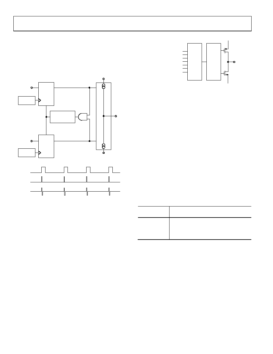
The PFD takes inputs from the R counter and N counter (N =
BP + A) and produces an output proportional to the phase and
frequency difference between them. Figure 25 is a simplified
schematic.
DELAY
ELEMENT
U3
CLR2
Q2
D2
U2
CLR1
Q1
D1
CHARGE
PUMP
DOWN
UP
HI
U1
R DIVIDER
N DIVIDER
CP OUTPUT
R DIVIDER
N DIVIDER
CP
CPGND
VP
01
036
-02
5
Figure 26. MUXOUT Circuit
LOCK DETECT
MUXOUT can be programmed for analog lock detect. The
N-channel open-drain analog lock detect is operated with an
external pull-up resistor of 10 kΩ nominal. When lock is
detected, it is high with narrow, low going pulses.
INPUT SHIFT REGISTER
The functional block diagram for the ADF420x family is shown
in Figure 1. The main blocks include a 22-bit input shift register,
a 14-bit R counter, and a 17-bit N counter, comprising a 6-bit
A counter and an 11-bit B counter. Data is clocked into the
22-bit shift register on each rising edge of CLK. The data is
clocked in MSB first. Data is transferred from the shift register
to one of four latches on the rising edge of LE. The destination
latch is determined by the state of the two control bits (C2, C1)
in the shift register. These are the two LSBs (DB1, DB0) as
shown in the timing diagram of Figure 2.
Table 5 is the truth table for these bits.
Table 5. C2, C1 Truth Table
Figure 25. PFD Simplified Schematic and Timing (In Lock)
The PFD includes a delay element that sets the width of the
antibacklash phase. The typical value for this in the ADF420x
family is 3 ns. The pulse ensures that there is no dead zone in
the PFD transfer function and minimizes phase noise and
reference spurs.
Control Bits
C2
C1
Data Latch
0
RF2 R counter
0
1
RF2 AB counter (and prescaler select)
1
0
RF1 R counter
1
RF1 AB counter (and prescaler select)
MUXOUT AND LOCK DETECT
The output multiplexer on the ADF4206 family allows the user
to access various internal points on the chip. The state of
MUXOUT is controlled by P3, P4, P11, and P12. See Figure 28
and Figure 30. Figure 26 shows the MUXOUT circuit in block
diagram form.
相关PDF资料 |
PDF描述 |
|---|---|
| ADF4001BCPZ-RL7 | IC CLOCK GEN PLL 200MHZ 20LFCSP |
| VI-B1K-MV-S | CONVERTER MOD DC/DC 40V 150W |
| ADF4001BRUZ-R7 | IC CLOCK GEN PLL 200MHZ 16TSSOP |
| VI-21K-MW-S | CONVERTER MOD DC/DC 40V 100W |
| VE-25T-IV | CONVERTER MOD DC/DC 6.5V 150W |
相关代理商/技术参数 |
参数描述 |
|---|---|
| ADF4210 | 制造商:AD 制造商全称:Analog Devices 功能描述:Dual RF/IF PLL Frequency Synthesizers |
| ADF4210BCP | 制造商:Rochester Electronics LLC 功能描述:- Bulk |
| ADF4210BRU | 制造商:Rochester Electronics LLC 功能描述:- Bulk 制造商:Analog Devices 功能描述: |
| ADF4211 | 制造商:AD 制造商全称:Analog Devices 功能描述:Dual RF/IF PLL Frequency Synthesizers |
| ADF4211BCP | 制造商:Rochester Electronics LLC 功能描述:- Bulk |
发布紧急采购,3分钟左右您将得到回复。