- 您现在的位置:买卖IC网 > PDF目录8912 > ADF4216BRU-REEL (Analog Devices Inc)IC PLL FREQ SYNTHESIZER 20-TSSOP PDF资料下载
参数资料
| 型号: | ADF4216BRU-REEL |
| 厂商: | Analog Devices Inc |
| 文件页数: | 11/20页 |
| 文件大小: | 0K |
| 描述: | IC PLL FREQ SYNTHESIZER 20-TSSOP |
| 产品变化通告: | ADF4213,16 Discontinuation 15/May/2012 |
| 标准包装: | 2,500 |
| 类型: | 时钟/频率合成器(RF/IF) |
| PLL: | 是 |
| 输入: | CMOS,TTL |
| 输出: | 时钟 |
| 电路数: | 1 |
| 比率 - 输入:输出: | 3:1 |
| 差分 - 输入:输出: | 是/无 |
| 频率 - 最大: | 1.2GHz |
| 除法器/乘法器: | 是/无 |
| 电源电压: | 2.7 V ~ 5.5 V |
| 工作温度: | -40°C ~ 85°C |
| 安装类型: | 表面贴装 |
| 封装/外壳: | 20-TSSOP(0.173",4.40mm 宽) |
| 供应商设备封装: | 20-TSSOP |
| 包装: | 带卷 (TR) |
REV. 0
ADF4216/ADF4217/ADF4218
–19–
INTERFACING
The ADF4216/ADF4217/ADF4218 family has a simple SPI-
compatible serial interface for writing to the device. SCLK,
SDATA, and LE (Latch Enable) control the data transfer. When
LE goes high, the 22 bits that have been clocked into the input
register on each rising edge of SCLK will be transferred to the
appropriate latch. See Figure 1 for the Timing Diagram and
Table I for the Latch Truth Table.
The maximum allowable serial clock rate is 20 MHz. This
means that the maximum update rate possible for the device is
909 kHz or one update every 1.1 ms. This is certainly more than
adequate for systems that will have typical lock times in hun-
dreds of microseconds.
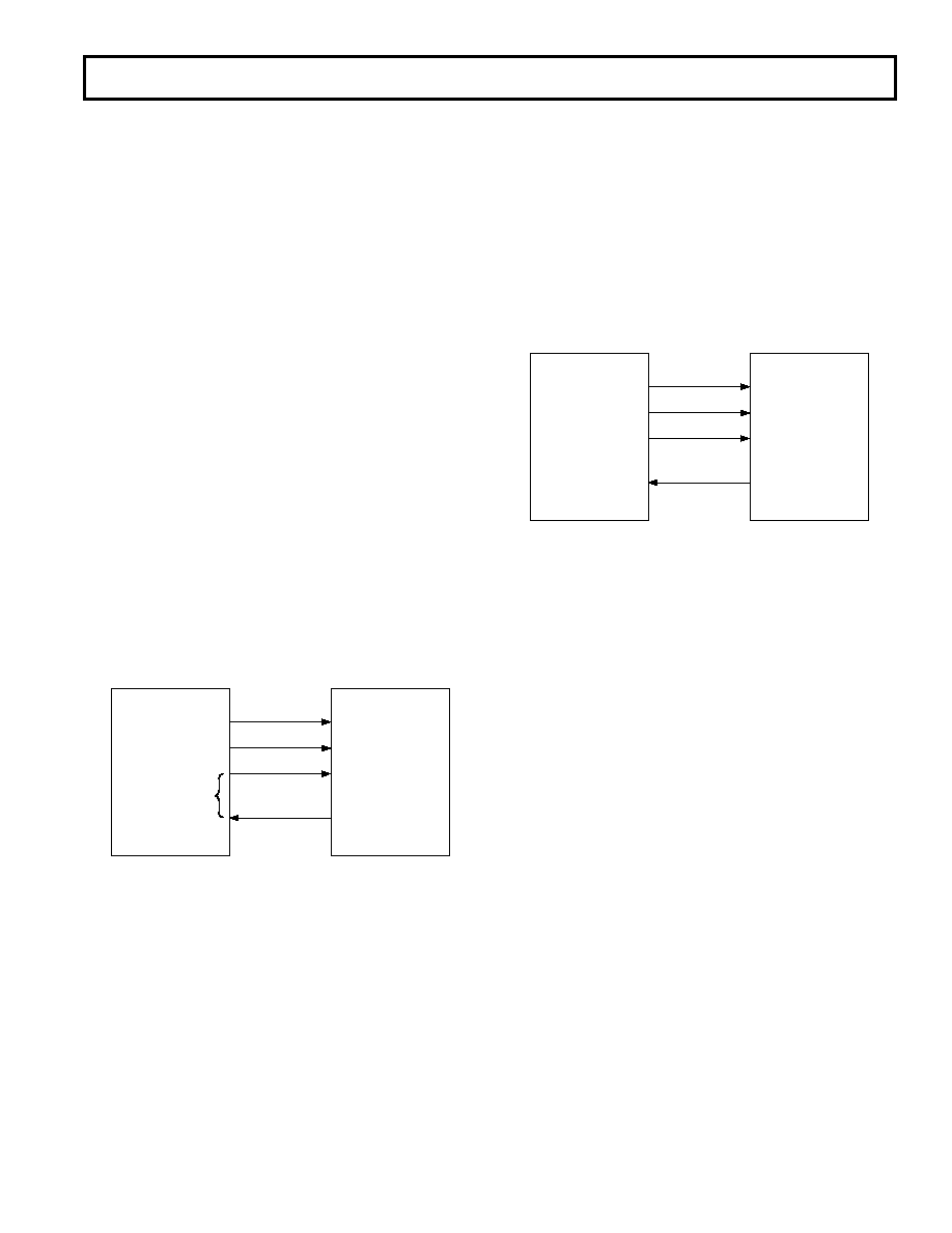
ADuC812 Interface
Figure 9 shows the interface between the ADF421x family and
the ADuC812 microconverter. Since the ADuC812 is based on
an 8051 core, this interface can be used with any 8051-based
microcontroller. The microconverter is set up for SPI Master
Mode with CPHA = 0. To initiate the operation, the I/O port
driving LE is brought low. Each latch of the ADF421x family
needs a 22-bit word. This is accomplished by writing three 8-bit
bytes from the microconverter to the device. When the third
byte has been written, the LE input should be brought high to
complete the transfer.
On rst applying power to the ADF421x family, it requires four
writes (one each to the R counter latch and the AB counter latch
for both RF1 and RF2 side) for the output to become active.
When operating in the mode described, the maximum SCLOCK
rate of the ADuC812 is 4 MHz. This means that the maximum
rate at which the output frequency can be changed will be about
180 kHz.
ADuC812
ADF4216/
ADF4217/
ADF4218
SCLK
SDATA
LE
MUXOUT
(LOCK DETECT)
SCLOCK
MOSI
I/O PORTS
Figure 9. ADuC812 to ADF421x Family Interface
ADSP-2181 Interface
Figure 10 shows the interface between the ADF421x family and
the ADSP-21xx Digital Signal Processor. As previously noted,
the ADF421x family needs a 22-bit serial word for each latch
write. The easiest way to accomplish this using the ADSP-21xx
family is to use the Autobuffered Transmit Mode of operation
with Alternate Framing. This provides a means for transmitting
an entire block of serial data before an interrupt is generated.
Set up the word length for eight bits and use three memory
locations for each 22-bit word. To program each 22-bit latch,
store the three 8-bit bytes, enable the Autobuffered mode and
then write to the transmit register of the DSP. This last opera-
tion initiates the autobuffer transfer.
ADSP-21xx
ADF4216/
ADF4217/
ADF4218
SCLK
SDATA
LE
MUXOUT
(LOCK DETECT)
SCLK
DT
I/O FLAG
TFS
Figure 10. ADSP-21xx to ADF421x Family Interface
相关PDF资料 |
PDF描述 |
|---|---|
| MS3102E36-17P | CONN RCPT 47POS BOX MNT W/PINS |
| ADF4213BRU-REEL | IC PLL FREQ SYNTHESIZER 20-TSSOP |
| GTC06AF-32-76S | CONN PLUG 19POS STRAIGHT W/SCKT |
| M83723/96W22196 | CONN PLUG 19POS STRAIGHT W/PINS |
| GTC00F-32-7P | CONN RCPT 35POS WALL MNT W/PINS |
相关代理商/技术参数 |
参数描述 |
|---|---|
| ADF4216BRU-REEL7 | 制造商:Analog Devices 功能描述:PLL Frequency Synthesizer Dual 20-Pin TSSOP T/R |
| ADF4216BRUZ | 制造商:Analog Devices 功能描述:Clock Synthesizer 5MHz to 1.2GHz 20-Pin TSSOP |
| ADF4216BRUZ-RL | 功能描述:IC PLL FREQ SYNTHESIZER 20TSSOP RoHS:是 类别:集成电路 (IC) >> 时钟/计时 - 时钟发生器,PLL,频率合成器 系列:- 产品变化通告:Product Discontinuation 04/May/2011 标准包装:96 系列:- 类型:时钟倍频器,零延迟缓冲器 PLL:带旁路 输入:LVTTL 输出:LVTTL 电路数:1 比率 - 输入:输出:1:8 差分 - 输入:输出:无/无 频率 - 最大:133.3MHz 除法器/乘法器:是/无 电源电压:3 V ~ 3.6 V 工作温度:0°C ~ 70°C 安装类型:表面贴装 封装/外壳:16-TSSOP(0.173",4.40mm 宽) 供应商设备封装:16-TSSOP 包装:管件 其它名称:23S08-5HPGG |
| ADF4216BRUZ-RL7 | 制造商:Analog Devices 功能描述:PLL Frequency Synthesizer Dual 20-Pin TSSOP T/R |
| ADF4217 | 制造商:AD 制造商全称:Analog Devices 功能描述:Dual RF PLL Frequency Synthesizers |
发布紧急采购,3分钟左右您将得到回复。