- 您现在的位置:买卖IC网 > PDF目录9221 > ADF4360-0BCPZ (Analog Devices Inc)IC INTEGRATED SYNTH/VCO 24-LFCSP PDF资料下载
参数资料
| 型号: | ADF4360-0BCPZ |
| 厂商: | Analog Devices Inc |
| 文件页数: | 8/24页 |
| 文件大小: | 0K |
| 描述: | IC INTEGRATED SYNTH/VCO 24-LFCSP |
| 标准包装: | 1 |
| 类型: | 扇出配送,整数-N,合成器(RF) |
| PLL: | 是 |
| 输入: | CMOS,TTL |
| 输出: | 时钟 |
| 电路数: | 1 |
| 比率 - 输入:输出: | 1:2 |
| 差分 - 输入:输出: | 无/无 |
| 频率 - 最大: | 2.725GHz |
| 除法器/乘法器: | 是/无 |
| 电源电压: | 3 V ~ 3.6 V |
| 工作温度: | -40°C ~ 85°C |
| 安装类型: | 表面贴装 |
| 封装/外壳: | 24-VFQFN 裸露焊盘,CSP |
| 供应商设备封装: | 24-LFCSP-VQ(4x4) |
| 包装: | 托盘 |
| 产品目录页面: | 551 (CN2011-ZH PDF) |
ADF4360-0
Data Sheet
Rev. C | Page 16 of 24
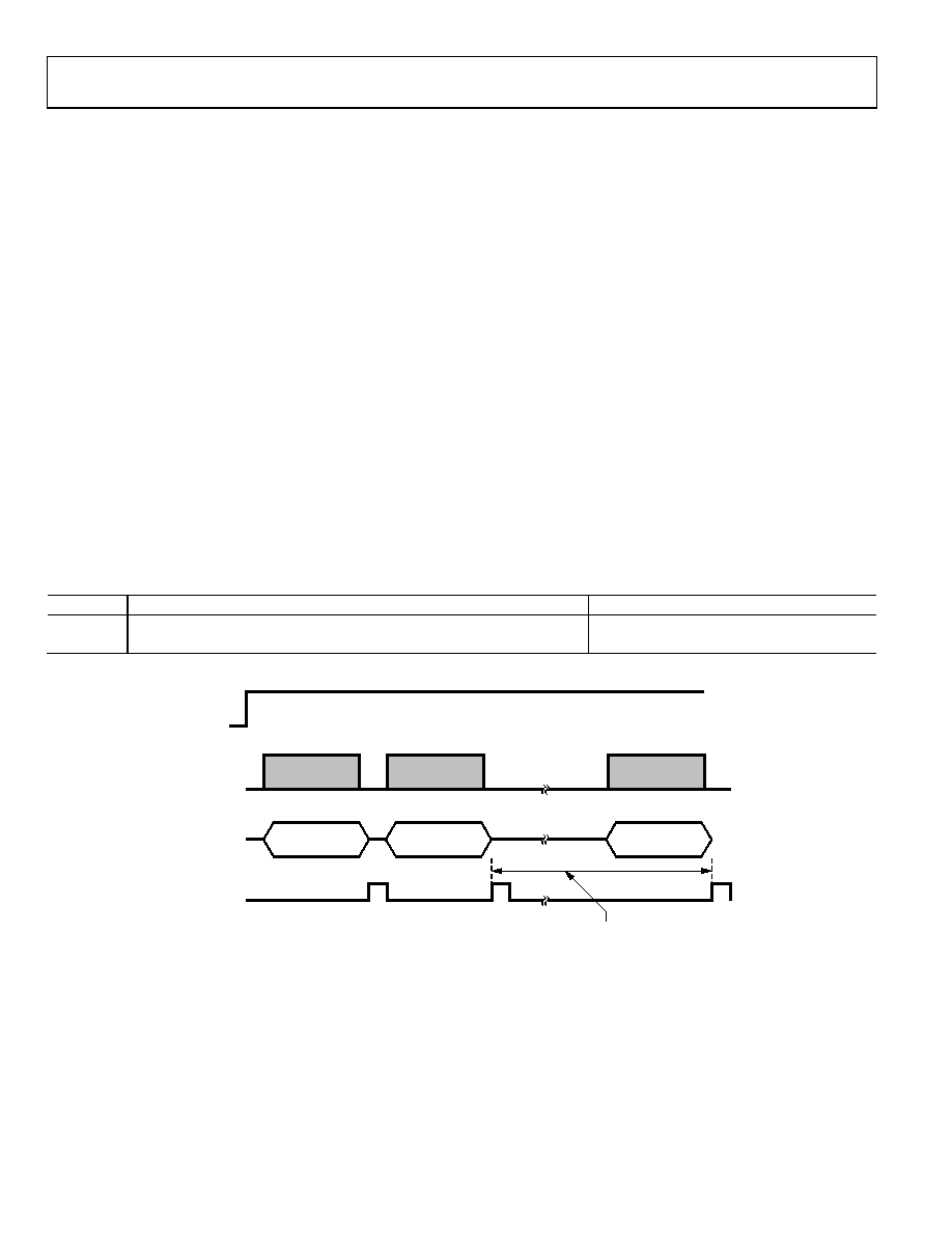
POWER-UP
Power-Up Sequence
The correct programming sequence for the ADF4360-0 after
power-up is:
1. R counter latch
2. Control latch
3. N counter latch
Initial Power-Up
Initial power-up refers to programming the part after the
application of voltage to the AVDD, DVDD, VVCO, and CE pins. On
initial power-up, an interval is required between programming
the control latch and programming the N counter latch.
This interval is necessary to allow the transient behavior of the
ADF4360-0 during initial power-up to have settled. During
initial power-up, a write to the control latch powers up the part
and the bias currents of the VCO begin to settle. If these cur-
rents have not settled to within 10% of their steady-state value
and if the N counter latch is then programmed, the VCO may
not be able to oscillate at the desired frequency, which does not
allow the band select logic to choose the correct frequency band
and the ADF4360-0 may not achieve lock. If the recommended
interval is inserted and the N counter latch is programmed, the
band select logic can choose the correct frequency band and the
part locks to the correct frequency.
This duration of this interval is affected by the value of the
capacitor on the CN pin (Pin 14). This capacitor is used to
reduce the close-in noise of the ADF4360-0 VCO. The recom-
mended value of this capacitor is 10 F. Using this value
requires an interval of ≥ 5 ms between the latching in of the
control latch bits and latching in of the N counter latch bits. If a
shorter delay is required, this capacitor can be reduced. A slight
phase noise penalty is incurred by this change, which is ex-
plained further in Table 10.
Table 10. CN Capacitance vs. Interval and Phase Noise
CN value
Recommended Interval between Control Latch and N Counter Latch
Open Loop Phase Noise @ 10 kHz Offset
10 F
≥ 5 ms
84 dBc
440 nF
≥ 600 s
82 dBc
CLOCK
POWER-UP
DATA
LE
R COUNTER
LATCH DATA
CONTROL
LATCH DATA
N COUNTER
LATCH DATA
REQUIRED INTERVAL
CONTROL LATCH WRITE TO
N COUNTER LATCH WRITE
04644-020
Figure 16. ADF4360-0 Power-Up Timing
相关PDF资料 |
PDF描述 |
|---|---|
| ADF4360-4BCPZ | IC INT SYNTH/VCO SEALED 24-LFCSP |
| ADF4360-7BCPZ | IC SYNTHESIZER/VCO 24-LFCSP |
| X9317WM8Z-2.7 | IC XDCP SGL 100TAP 10K 8-MSOP |
| SY89228UMG | IC CLK DIVIDER /3/5 LVPECL 16MLF |
| VE-JVX-MZ-S | CONVERTER MOD DC/DC 5.2V 25W |
相关代理商/技术参数 |
参数描述 |
|---|---|
| ADF4360-0BCPZ | 制造商:Analog Devices 功能描述:IC FREQ SYNTHESIZER |
| ADF4360-0BCPZRL | 功能描述:IC SYNTHESIZER VCO 24LFCSP RoHS:是 类别:集成电路 (IC) >> 时钟/计时 - 时钟发生器,PLL,频率合成器 系列:- 标准包装:1,000 系列:Precision Edge® 类型:时钟/频率合成器 PLL:无 输入:CML,PECL 输出:CML 电路数:1 比率 - 输入:输出:2:1 差分 - 输入:输出:是/是 频率 - 最大:10.7GHz 除法器/乘法器:无/无 电源电压:2.375 V ~ 3.6 V 工作温度:-40°C ~ 85°C 安装类型:表面贴装 封装/外壳:16-VFQFN 裸露焊盘,16-MLF? 供应商设备封装:16-MLF?(3x3) 包装:带卷 (TR) 其它名称:SY58052UMGTRSY58052UMGTR-ND |
| ADF4360-0BCPZRL7 | 功能描述:IC SYNTHESIZER VCO 24LFCSP RoHS:是 类别:集成电路 (IC) >> 时钟/计时 - 时钟发生器,PLL,频率合成器 系列:- 标准包装:1,000 系列:Precision Edge® 类型:时钟/频率合成器 PLL:无 输入:CML,PECL 输出:CML 电路数:1 比率 - 输入:输出:2:1 差分 - 输入:输出:是/是 频率 - 最大:10.7GHz 除法器/乘法器:无/无 电源电压:2.375 V ~ 3.6 V 工作温度:-40°C ~ 85°C 安装类型:表面贴装 封装/外壳:16-VFQFN 裸露焊盘,16-MLF? 供应商设备封装:16-MLF?(3x3) 包装:带卷 (TR) 其它名称:SY58052UMGTRSY58052UMGTR-ND |
| ADF4360-1 | 制造商:AD 制造商全称:Analog Devices 功能描述:Integrated Synthesizer and VCO |
| ADF4360-1_12 | 制造商:AD 制造商全称:Analog Devices 功能描述:Integrated Synthesizer and VCO |
发布紧急采购,3分钟左右您将得到回复。