参数资料
| 型号: | ADF4360-2BCPZRL7 |
| 厂商: | Analog Devices Inc |
| 文件页数: | 15/24页 |
| 文件大小: | 0K |
| 描述: | IC SYNTHESIZER VCO 24LFCSP |
| 标准包装: | 1,500 |
| 类型: | 扇出配送,整数-N,合成器(RF) |
| PLL: | 是 |
| 输入: | CMOS,TTL |
| 输出: | 时钟 |
| 电路数: | 1 |
| 比率 - 输入:输出: | 1:2 |
| 差分 - 输入:输出: | 无/无 |
| 频率 - 最大: | 2.17GHz |
| 除法器/乘法器: | 是/无 |
| 电源电压: | 3 V ~ 3.6 V |
| 工作温度: | -40°C ~ 85°C |
| 安装类型: | 表面贴装 |
| 封装/外壳: | 24-VFQFN 裸露焊盘,CSP |
| 供应商设备封装: | 24-LFCSP-VQ(4x4) |
| 包装: | 带卷 (TR) |
| 配用: | EVAL-ADF4360-2EBZ1-ND - BOARD EVALUATION FOR ADF4360-2 |
ADF4360-2
Data Sheet
Rev. C | Page 22 of 24
PCB DESIGN GUIDELINES FOR CHIP SCALE PACKAGE
The leads on the chip scale package (CP-24) are rectangular.
The printed circuit board pad for these should be 0.1 mm
longer than the package lead length and 0.05 mm wider than
the package lead width. The lead should be centered on the pad
to ensure that the solder joint size is maximized.
The bottom of the chip scale package has a central thermal pad.
The thermal pad on the printed circuit board should be at least
as large as this exposed pad. On the printed circuit board, there
should be a clearance of at least 0.25 mm between the thermal
pad and the inner edges of the pad pattern to ensure that
shorting is avoided.
Thermal vias can be used on the printed circuit board thermal
pad to improve thermal performance of the package. If vias are
used, they should be incorporated into the thermal pad at a
1.2 mm pitch grid. The via diameter should be between 0.3 mm
and 0.33 mm, and the via barrel should be plated with 1 ounce
of copper to plug the via.
The user should connect the printed circuit thermal pad to
AGND. This is internally connected to AGND.
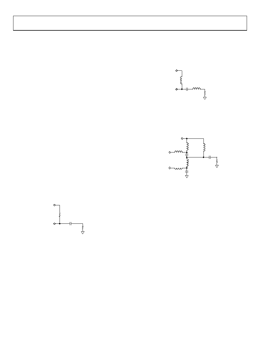
OUTPUT MATCHING
There are a number of ways to match the output of the
ADF4360-2 for optimum operation; the most basic is to use a
50 resistor to VVCO. A dc bypass capacitor of 100 pF is
connected in series, as shown in Figure 21. Because the resistor
is not frequency dependent, this provides a good broadband
match. The output power in this circuit typically gives 6 dBm
output power into a 50 load.
100pF
04436-
025
RFOUT
VVCO
50
51
Figure 21. Simple ADF4360-2 Output Stage
A better solution is to use a shunt inductor (acting as an RF
choke) to VVCO. This gives a better match and, therefore, more
output power. Additionally, a series inductor is added after the
dc bypass capacitor to provide a resonant LC circuit. This tunes
the oscillator output and provides approximately 10 dB
additional rejection of the second harmonic. The shunt
inductor needs to be a relatively high value (>40 nH).
Experiments have shown that the circuit shown in Figure 22
provides an excellent match to 50 over the operating range of
the ADF4360-2. This gives approximately 3 dBm output
power across the frequency range of the ADF4360-2. Both
single-ended architectures can be examined using the
EV-ADF4360-2EB1Z evaluation board.
3.6nH
47nH
1.8pF
04436-
026
RFOUT
VVCO
50
Figure 22. Optimum ADF4360-2 Output Stage
If the user does not need the differential outputs available on
the ADF4360-2, the user can either terminate the unused
output or combine both outputs using a balun. The circuit in
Figure 23 shows how best to combine the outputs.
2.2nH
3.6nH
47nH
3.6nH
1.8pF
10pF
1.8pF
50
2.2nH
RFOUTA
VVCO
RFOUTB
04436-
027
Figure 23. Balun for Combining ADF4360-2 RF Outputs
The circuit in Figure 23 is a lumped-lattice-type LC balun. It is
designed for a center frequency of 2.0 GHz and outputs 2.0 dBm at
this frequency. The series 2.2 nH inductor is used to tune out
any parasitic capacitance due to the board layout from each
input, and the remainder of the circuit is used to shift the
output of one RF input by +90° and the second by 90°, thus
combining the two. The action of the 3.6 nH inductor and the
1.8 pF capacitor accomplishes this. The 47 nH is used to
provide an RF choke to feed the supply voltage, and the 10 pF
capacitor provides the necessary dc block. To ensure good RF
performance, the circuits in Figure 22 and Figure 23 are
implemented with Coilcraft 0402/0603 inductors and AVX 0402
thin-film capacitors.
Alternatively, instead of the LC balun shown in Figure 23, both
outputs can be combined using a 180° rat-race coupler.
相关PDF资料 |
PDF描述 |
|---|---|
| ADF4360-3BCPZRL7 | IC SYNTHESIZER VCO 24LFCSP |
| ADF4360-4BCPZRL7 | IC SYNTHESIZER VCO 24LFCSP |
| ADF4360-5BCPZRL7 | IC SYNTHESIZER VCO 24LFCSP |
| ADF4360-6BCPZRL7 | IC SYNTHESIZER VCO 24LFCSP |
| ADF4360-7BCPZRL7 | IC SYNTHESIZER VCO 24LFCSP |
相关代理商/技术参数 |
参数描述 |
|---|---|
| ADF4360-3 | 制造商:AD 制造商全称:Analog Devices 功能描述:Integrated Synthesizer and VCO |
| ADF4360-3BCP | 制造商:Analog Devices 功能描述:PLL Frequency Synthesizer Single 24-Pin LFCSP EP 制造商:Rochester Electronics LLC 功能描述:INT. SYNTHESIZER & VCO - 1600 - 1950 MHZ - Bulk 制造商:Analog Devices 功能描述:IC SYNTHESIZER PLL |
| ADF4360-3BCPRL | 制造商:Analog Devices 功能描述:PLL Frequency Synthesizer Single 24-Pin LFCSP EP T/R |
| ADF4360-3BCPRL7 | 制造商:Analog Devices 功能描述:PLL Frequency Synthesizer Single 24-Pin LFCSP EP T/R |
| ADF4360-3BCPU1 | 制造商:Analog Devices 功能描述:PLL FREQ SYNTHESIZER SGL 24LFCSP EP - Bulk |
发布紧急采购,3分钟左右您将得到回复。