- 您现在的位置:买卖IC网 > PDF目录11490 > ADG1209YCPZ-REEL7 (Analog Devices Inc)IC MULTIPLEXER DUAL 4X1 16LFCSP PDF资料下载
参数资料
| 型号: | ADG1209YCPZ-REEL7 |
| 厂商: | Analog Devices Inc |
| 文件页数: | 20/20页 |
| 文件大小: | 0K |
| 描述: | IC MULTIPLEXER DUAL 4X1 16LFCSP |
| 产品培训模块: | iCMOS™ Switches and Multiplexers for Data Acquisition Switch Fundamentals |
| 设计资源: | Parametric Measurement Unit and Supporting Components for PAD Appls Using AD5522 and AD7685 (CN0104) |
| 标准包装: | 1 |
| 系列: | iCMOS® |
| 功能: | 多路复用器 |
| 电路: | 2 x 4:1 |
| 导通状态电阻: | 475 欧姆 |
| 电压电源: | 单/双电源 |
| 电压 - 电源,单路/双路(±): | 12V,±15V |
| 电流 - 电源: | 220µA |
| 工作温度: | -40°C ~ 125°C |
| 安装类型: | 表面贴装 |
| 封装/外壳: | 16-VQFN 裸露焊盘,CSP |
| 供应商设备封装: | 16-LFCSP-VQ EP(4x4) |
| 包装: | 标准包装 |
| 产品目录页面: | 789 (CN2011-ZH PDF) |
| 其它名称: | ADG1209YCPZ-REEL7DKR |
ADG1208/ADG1209
Rev. B | Page 9 of 20
1
2
3
4
5
6
7
8
16
15
14
13
12
EN
VSS
S1A
S2A
A0
GND
VDD
S1B
S2B
A1
ADG1209
TOP VIEW
(Not to Scale)
11
10
9
S4A
S3A
S4B
DA
DB
S3B
0
57
13
-00
3
PIN 1
INDICATOR
1
VSS
2
S1A
3
S2A
4
S3A
11 S1B
12 VDD
10 S2B
9S3B
15
A
0
16
E
N
14
A
1
13
G
N
D
TOP VIEW
(Not to Scale)
ADG1209
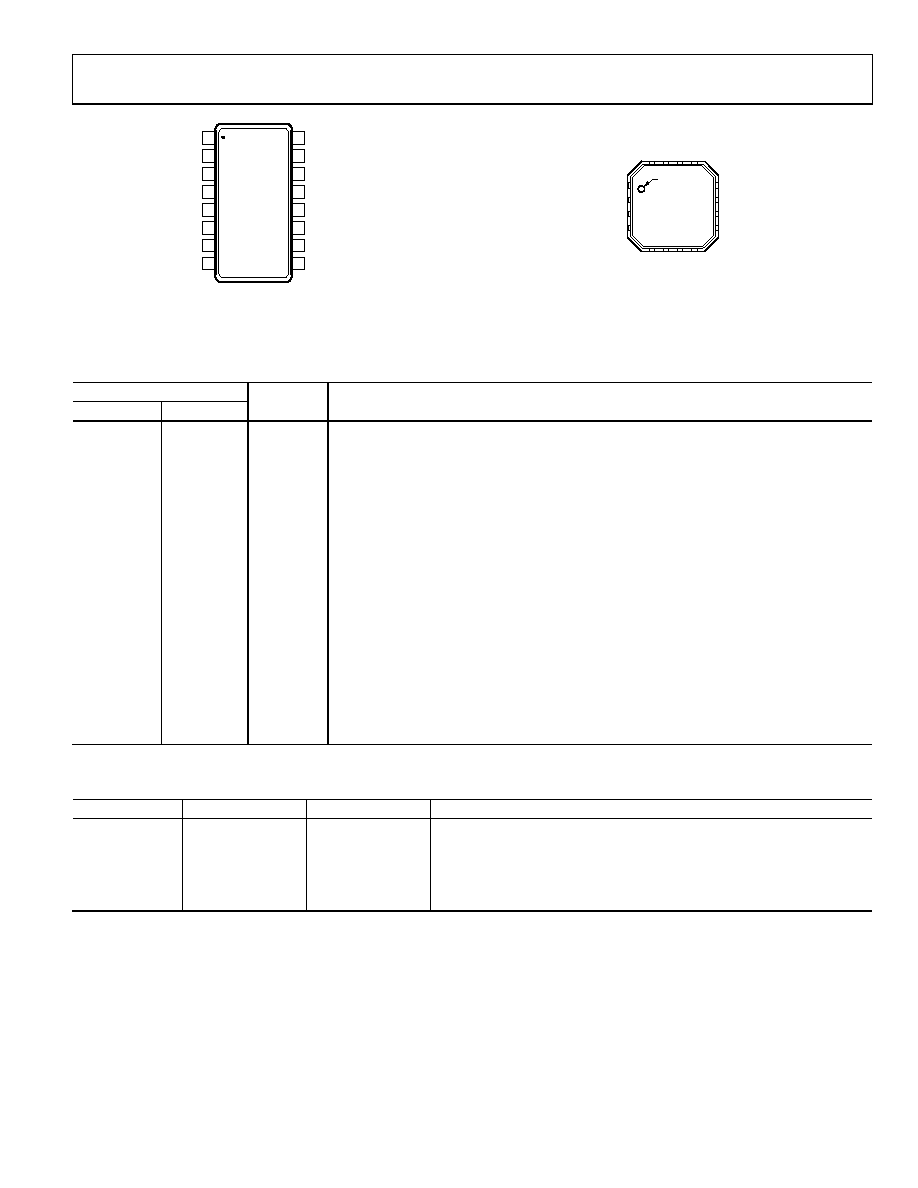
Figure 5. ADG1209 Pin Configuration (TSSOP/SOIC)
5
S
4
A
6
D
A
7
D
B
8
S
4B
05
71
3-
00
5
Figure 6. ADG1209 Pin Configurations (LFCSP_VQ),
Exposed Pad Tied to Substrate, VSS
Table 6. ADG1209 Pin Function Descriptions
Pin Number
TSSOP/SOIC
LFCSP_VQ
Mnemonic
Description
1
15
A0
Logic Control Input.
2
16
EN
Active High Digital Input. When low, the device is disabled and all switches are off.
When high, Ax logic inputs determine on switches.
3
1
VSS
Most Negative Power Supply Potential. In single-supply applications, it can be
connected to ground.
4
2
S1A
Source Terminal 1A. Can be an input or an output.
5
3
S2A
Source Terminal 2A. Can be an input or an output.
6
4
S3A
Source Terminal 3A. Can be an input or an output.
7
5
S4A
Source Terminal 4A. Can be an input or an output.
8
6
DA
Drain Terminal A. Can be an input or an output.
9
7
DB
Drain Terminal B. Can be an input or an output.
10
8
S4B
Source Terminal 4B. Can be an input or an output.
11
9
S3B
Source Terminal 3B. Can be an input or an output.
12
10
S2B
Source Terminal 2B. Can be an input or an output.
13
11
S1B
Source Terminal 1B. Can be an input or an output.
14
12
VDD
Most Positive Power Supply Potential.
15
13
GND
Ground (0 V) Reference.
16
14
A1
Logic Control Input.
Table 7. ADG1209 Truth Table
A1
A0
EN
On Switch Pair
X
0
None
0
1
0
1
2
1
0
1
3
1
4
相关PDF资料 |
PDF描述 |
|---|---|
| VI-BNK-CU-F3 | CONVERTER MOD DC/DC 40V 200W |
| VI-BNK-CU-F1 | CONVERTER MOD DC/DC 40V 200W |
| PIC18LF45J11T-I/ML | IC PIC MCU FLASH 32KB 44-QFN |
| ADG419BRZ-REEL7 | IC SWITCH SPDT 8SOIC |
| PIC18LF26K80T-I/SO | MCU PIC 64KB FLASH 28SOIC |
相关代理商/技术参数 |
参数描述 |
|---|---|
| ADG1209YCPZ-REEL71 | 制造商:AD 制造商全称:Analog Devices 功能描述:Low Capacitance, 4-/8-Channel 15 V/12 V iCMOS Multiplexers |
| ADG1209YRUZ | 功能描述:IC MULTIPLEXER 15V 4:1 16TSSOP RoHS:是 类别:集成电路 (IC) >> 接口 - 模拟开关,多路复用器,多路分解器 系列:iCMOS® 特色产品:MicroPak? 标准包装:1 系列:- 功能:开关 电路:2 x SPST - NC 导通状态电阻:500 毫欧 电压电源:单电源 电压 - 电源,单路/双路(±):1.4 V ~ 4.3 V 电流 - 电源:150nA 工作温度:-40°C ~ 125°C 安装类型:表面贴装 封装/外壳:8-XFDFN 供应商设备封装:8-XSON,SOT833-1 (1.95x1) 包装:Digi-Reel® 其它名称:568-5557-6 |
| ADG1209YRUZ1 | 制造商:AD 制造商全称:Analog Devices 功能描述:Low Capacitance, 4-/8-Channel 15 V/12 V iCMOS Multiplexers |
| ADG1209YRUZ-REEL7 | 功能描述:IC MULTIPLEXER 15V 4:1 16TSSOP RoHS:是 类别:集成电路 (IC) >> 接口 - 模拟开关,多路复用器,多路分解器 系列:iCMOS® 其它有关文件:STG4159 View All Specifications 标准包装:5,000 系列:- 功能:开关 电路:1 x SPDT 导通状态电阻:300 毫欧 电压电源:双电源 电压 - 电源,单路/双路(±):±1.65 V ~ 4.8 V 电流 - 电源:50nA 工作温度:-40°C ~ 85°C 安装类型:表面贴装 封装/外壳:7-WFBGA,FCBGA 供应商设备封装:7-覆晶 包装:带卷 (TR) |
| ADG1209YRUZ-REEL71 | 制造商:AD 制造商全称:Analog Devices 功能描述:Low Capacitance, 4-/8-Channel 15 V/12 V iCMOS Multiplexers |
发布紧急采购,3分钟左右您将得到回复。