- 您现在的位置:买卖IC网 > PDF目录11481 > ADG1439BRUZ (Analog Devices Inc)IC MULTIPLEXER DL 4X1 20TSSOP PDF资料下载
参数资料
| 型号: | ADG1439BRUZ |
| 厂商: | Analog Devices Inc |
| 文件页数: | 11/20页 |
| 文件大小: | 0K |
| 描述: | IC MULTIPLEXER DL 4X1 20TSSOP |
| 标准包装: | 75 |
| 系列: | iCMOS® |
| 功能: | 多路复用器 |
| 电路: | 2 x 4:1 |
| 导通状态电阻: | 21.5 欧姆 |
| 电压电源: | 单/双电源 |
| 电压 - 电源,单路/双路(±): | 5 V ~ 16.5 V,±2.25 V ~ 8.25 V |
| 电流 - 电源: | 1nA |
| 工作温度: | -40°C ~ 125°C |
| 安装类型: | 表面贴装 |
| 封装/外壳: | 20-TSSOP(0.173",4.40mm 宽) |
| 供应商设备封装: | 20-TSSOP |
| 包装: | 管件 |
| 产品目录页面: | 802 (CN2011-ZH PDF) |
ADG1438/ADG1439
Rev. A | Page 19 of 20
THEORY OF OPERATION
The ADG1438 and ADG1439 are serially controlled, 8-channel
and dual 4-channel matrix switches, respectively. While
providing the normal multiplexing and demultiplexing
functions, these devices also provide the user with more
flexibility as to where a signal can be routed. Each of the eight
bits of the 8-bit write corresponds to one switch of the device.
Logic 1 in a particular bit position turns the switch on, whereas
Logic 0 turns the switch off. Because each switch is
independently controlled by an individual bit, this provides the
option of having any, all, or none of the switches on. This
feature may be particularly useful in the demultiplexing
application where the user may wish to direct one signal from
the drain to a number of outputs (sources). Care must be taken,
however, in the multiplexing situation where a number of
inputs may be shorted together (separated only by the small on
resistance of the switch).
SERIAL INTERFACE
The ADG1438/ADG1439 has a 3-wire serial interface (SYNC,
SCLK, and DIN pins) that is compatible with SPI, QSPI, and
MICROWIRE interface standards, as well as most DSPs (see
for a timing diagram of a typical write sequence).
The write sequence begins by bringing the SYNC line low. This
enables the input shift register. Data from the DIN line is clocked
into the 8-bit input shift register on the falling edge of SCLK.
The serial clock frequency can be as high as 50 MHz, making
the ADG1438/ADG1439 compatible with high speed DSPs.
Data can be written to the shift register in more or fewer than
eight bits. In each case, the shift register retains the last eight
bits that are written. When all eight bits are written into the
shift register, the SYNC line is brought high again. The switches
are updated with the new configuration, and the input shift
register is disabled. With SYNC held high, the input shift
register is disabled so that further data or noise on the DIN line
has no effect on the shift register.
Data appears on the SDO pin on the rising edge of SCLK,
suitable for daisy-chaining or readback, delayed by eight bits.
INPUT SHIFT REGISTER
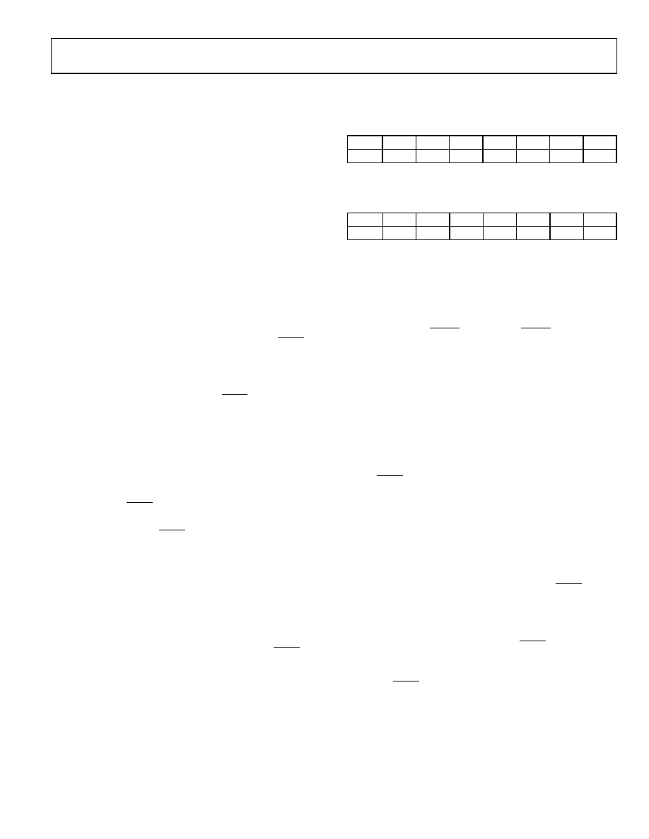
The input shift register is eight bits wide, as shown in Table 12 and
Table 13. Each bit controls one switch. These data bits are
transferred to the switch register on the rising edge of SYNC.
Table 12. ADG1438 Input Shift Register Bit Map1
MSB
LSB
DB7
DB6
DB5
DB4
DB3
DB2
DB1
DB0
S8
S7
S6
S5
S4
S3
S2
S1
1 Logic 0 = switch off, and Logic 1 = switch on.
Table 13. ADG1439 Input Shift Register Bit Map1
MSB
LSB
DB7
DB6
DB5
DB4
DB3
DB2
DB1
DB0
S4B
S3B
S2B
S1B
S4A
S3A
S2A
S1A
1 Logic 0 = switch off, and Logic 1 = switch on.
POWER-ON RESET
The ADG1438/ADG1439 contain a power-on reset circuit. On
power-up of the device, all switches are off, and the internal
shift register is filled with zeros and remains so until a valid
write takes place.
The part also has a RESET pin. When the RESET pin is low, all
switches are off, and the appropriate registers are cleared to 0.
DAISY-CHAINING
For systems that contain several switches, the SDO pin can be
used to daisy-chain several devices together. The SDO pin can
also be used for diagnostic purposes and to provide serial
readback where the user wants to read back the switch contents.
The SDO pin is an open-drain output that should be pulled to
the VL supply with an external resistor.
The SCLK is continuously applied to the input shift register
when SYNC is low. If more than eight clock pulses are applied,
the data ripples out of the shift register and appears on the SDO
line. This data is clocked out on the rising edge of SCLK and is
valid on the falling edge. By connecting this line to the DIN
input on the next switch in the chain, a multiswitch interface is
constructed. Each switch in the system requires eight clock
pulses; therefore, the total number of clock cycles must equal
8N, where N is the total number of devices in the chain.
When the serial transfer to all devices is complete, SYNC is
taken high. This prevents any further data from being clocked
into the input shift register.
The serial clock can be a continuous or a gated clock. A con-
tinuous SCLK source can be used only if SYNC can be held low
for the correct number of clock cycles. In gated clock mode, a
burst clock containing the exact number of clock cycles must be
used, and SYNC must be taken high after the final clock to latch
the data. Gated clock mode reduces power consumption by
reducing the active clock time.
相关PDF资料 |
PDF描述 |
|---|---|
| ADG1234YRUZ | IC SWITCH QUAD SPDT 20TSSOP |
| VE-BND-CU-F2 | CONVERTER MOD DC/DC 85V 200W |
| ADG201HSJNZ | IC SWITCH QUAD SPST 16DIP |
| VE-B6L-CU-F3 | CONVERTER MOD DC/DC 28V 200W |
| PIC16LC57CT-04I/SS | IC MCU OTP 2KX12 28SSOP |
相关代理商/技术参数 |
参数描述 |
|---|---|
| ADG1439BRUZ-REEL7 | 功能描述:IC MULTIPLEXER DL 4X1 20TSSOP RoHS:是 类别:集成电路 (IC) >> 接口 - 模拟开关,多路复用器,多路分解器 系列:iCMOS® 其它有关文件:STG4159 View All Specifications 标准包装:5,000 系列:- 功能:开关 电路:1 x SPDT 导通状态电阻:300 毫欧 电压电源:双电源 电压 - 电源,单路/双路(±):±1.65 V ~ 4.8 V 电流 - 电源:50nA 工作温度:-40°C ~ 85°C 安装类型:表面贴装 封装/外壳:7-WFBGA,FCBGA 供应商设备封装:7-覆晶 包装:带卷 (TR) |
| ADG1517 | 制造商:AD 制造商全称:Analog Devices 功能描述:1.6 Ω On Resistance, 15 V iCMOS SPST Switch |
| ADG1517BCPZ-REEL7 | 功能描述:IC SWITCH SPST 8LFCSP RoHS:是 类别:集成电路 (IC) >> 接口 - 模拟开关,多路复用器,多路分解器 系列:iCMOS® 标准包装:1 系列:- 功能:开关 电路:2 x SPST - NC/NO 导通状态电阻:8 欧姆 电压电源:单电源 电压 - 电源,单路/双路(±):2.3 V ~ 4.3 V 电流 - 电源:1µA 工作温度:-40°C ~ 85°C 安装类型:表面贴装 封装/外壳:8-UFQFN 供应商设备封装:8-迷你型QFN(1.4x1.4) 包装:剪切带 (CT) 其它名称:DG2738DN-T1-E4CT |
| ADG1604 | 制造商:AD 制造商全称:Analog Devices 功能描述:1 Ω Typical On Resistance, ±5 V, +12 V, +5 V, and +3.3 V, 4:1 Multiplexer |
| ADG1604BCPZ-REEL | 功能描述:IC MULTIPLEXER 4X1 16LFCSP RoHS:是 类别:集成电路 (IC) >> 接口 - 模拟开关,多路复用器,多路分解器 系列:- 标准包装:1,000 系列:- 功能:多路复用器 电路:1 x 4:1 导通状态电阻:- 电压电源:双电源 电压 - 电源,单路/双路(±):±5V 电流 - 电源:7mA 工作温度:-40°C ~ 85°C 安装类型:表面贴装 封装/外壳:16-SOIC(0.154",3.90mm 宽) 供应商设备封装:16-SOIC 包装:带卷 (TR) |
发布紧急采购,3分钟左右您将得到回复。