- 您现在的位置:买卖IC网 > PDF目录11217 > ADG5433BRUZ (Analog Devices Inc)IC SWITCH THREE SPST 16TSSOP PDF资料下载
参数资料
| 型号: | ADG5433BRUZ |
| 厂商: | Analog Devices Inc |
| 文件页数: | 3/24页 |
| 文件大小: | 0K |
| 描述: | IC SWITCH THREE SPST 16TSSOP |
| 标准包装: | 96 |
| 功能: | 开关 |
| 电路: | 3 x SPDT - NC/NO |
| 导通状态电阻: | 16 欧姆 |
| 电压电源: | 单/双电源 |
| 电压 - 电源,单路/双路(±): | 9 V ~ 40 V,±9 V ~ ±22 V |
| 电流 - 电源: | 80µA |
| 工作温度: | -40°C ~ 125°C |
| 安装类型: | 表面贴装 |
| 封装/外壳: | 16-TSSOP(0.173",4.40mm 宽) |
| 供应商设备封装: | 16-TSSOP |
| 包装: | 管件 |
Data Sheet
ADG5433/ADG5434
Rev. C | Page 11 of 24
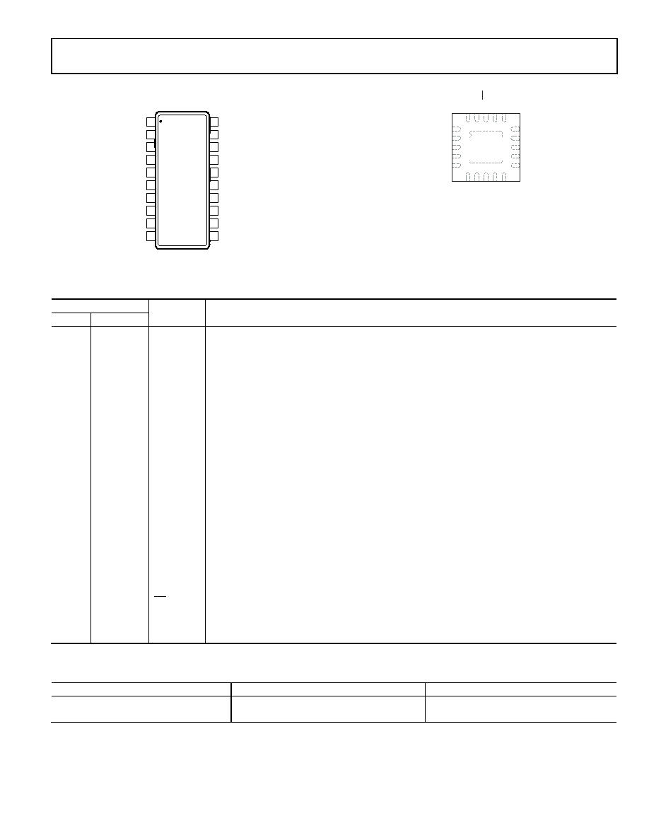
Figure 5. ADG5434 TSSOP Pin Configuration
Figure 6. ADG5434 LFCSP_WQ Pin Configuration
Table 10. ADG5434 Pin Function Descriptions
Pin No.
Mnemonic
Description
TSSOP
LFCSP_WQ
1
19
IN1
Logic Control Input 1.
2
20
S1A
Source Terminal 1A. This pin can be an input or an output.
3
1
D1
Drain Terminal 1. This pin can be an input or an output.
4
2
S1B
Source Terminal 1B. This pin can be an input or an output.
5
3
VSS
Most Negative Power Supply Potential. In single-supply applications, this pin can be connected to
ground.
6
4
GND
Ground (0 V) Reference.
7
5
S2B
Source Terminal 2B. This pin can be an input or an output.
8
6
D2
Drain Terminal 2. This pin can be an input or an output.
9
7
S2A
Source Terminal 2A. This pin can be an input or an output.
10
8
IN2
Logic Control Input 2.
11
9
IN3
Logic Control Input 3.
12
10
S3A
Source Terminal 3A. This pin can be an input or an output.
13
11
D3
Drain Terminal 3. This pin can be an input or an output.
14
12
S3B
Source Terminal 3B. This pin can be an input or an output.
15
N/A
NC
No Connect.
16
13
VDD
Most Positive Power Supply Potential.
17
14
S4B
Source Terminal 4B. This pin can be an input or an output.
18
15
D4
Drain Terminal 4. This pin can be an input or an output.
19
16
S4A
Source Terminal 4A. This pin can be an input or an output.
20
17
IN4
Logic Control Input 4.
N/A
18
EN
Active Low Digital Input. When high, the device is disabled and all switches are off. When low, INx
logic inputs determine the on switches.
N/A
EP
Exposed
Pad
The exposed pad is connected internally. For increased reliability of the solder joints and maximum
thermal capability, it is recommended that the pad be soldered to the substrate, VSS.
Table 11. ADG5434 Truth Table
INx
SxA
SxB
0
Off
On
1
On
Off
1
2
3
4
5
6
8
20
19
18
17
16
15
13
S1A
D1
S1B
7
S2B
GND
VSS
IN1
S4A
D4
S4B
14
S3B
9
S2A
12
S3A
10
IN2
11
IN3
D2
D3
NC
VDD
IN4
ADG5434
TOP VIEW
(Not to Scale)
NC = NO CONNECT
09
20
7-
004
D1
S1B
VSS
GND
S2B
VDD
S4B
D4
S3B
D3
D
2
S
2
A
IN
2
S
3
A
IN
3
E
N
IN
1
S
1
A
IN
4
S
4
A
09
207-
006
14
13
12
1
3
4
15
11
2
5
7
6
8
9
1
0
1
9
2
0
1
8
1
7
1
6
ADG5434
TOP VIEW
(Not to Scale)
NOTES
1. THE EXPOSED PAD IS CONNECTED INTERNALLY.
FOR INCREASED RELIABILITY OF THE SOLDER
JOINTS AND MAXIMUM THERMAL CAPABILITY,
IT IS RECOMMENDED THAT THE PAD BE
SOLDERED TO THE SUBSTRATE, VSS.
相关PDF资料 |
PDF描述 |
|---|---|
| VE-B2W-IX-F4 | CONVERTER MOD DC/DC 5.5V 75W |
| VE-BWR-IX | CONVERTER MOD DC/DC 7.5V 75W |
| 2225PC684MAT1A | CAP CER 0.68UF 250V 20% X7R 2225 |
| VE-B2W-IX-F3 | CONVERTER MOD DC/DC 5.5V 75W |
| VE-BWR-IW | CONVERTER MOD DC/DC 7.5V 100W |
相关代理商/技术参数 |
参数描述 |
|---|---|
| ADG5433BRUZ-REEL7 | 功能描述:模拟开关 IC Triple SPDT & Quad SPDT Latch up proof M RoHS:否 制造商:Texas Instruments 开关数量:2 开关配置:SPDT 开启电阻(最大值):0.1 Ohms 切换电压(最大): 开启时间(最大值): 关闭时间(最大值): 工作电源电压:2.7 V to 4.5 V 最大工作温度:+ 85 C 安装风格:SMD/SMT 封装 / 箱体:DSBGA-16 |
| ADG5433WBRUZ | 制造商:Analog Devices 功能描述:TRIPLE SPDT & QUAD SPDT LATCH UP PROOF M - Rail/Tube |
| ADG5434 | 制造商:AD 制造商全称:Analog Devices 功能描述:High Voltage Latch-Up Proof, Triple/Quad SPDT Switches |
| ADG5434BCPZ-REEL7 | 制造商:Analog Devices 功能描述:TRIPLE SPDT & QUAD SPDT LATCH UP PROOF M - Tape and Reel 制造商:Analog Devices 功能描述:IC SW ANLG QUAD SPDT 20LFCSP 制造商:Analog Devices 功能描述:Triple SPDT & Quad SPDT Latch up proof M |
| ADG5434BRUZ | 功能描述:IC SWITCH QUAD SPST 20TSSOP RoHS:是 类别:集成电路 (IC) >> 接口 - 模拟开关,多路复用器,多路分解器 系列:- 应用说明:Ultrasound Imaging Systems Application Note 产品培训模块:Lead (SnPb) Finish for COTS Obsolescence Mitigation Program 标准包装:250 系列:- 功能:开关 电路:单刀单掷 导通状态电阻:48 欧姆 电压电源:单电源 电压 - 电源,单路/双路(±):2.7 V ~ 5.5 V 电流 - 电源:5µA 工作温度:0°C ~ 70°C 安装类型:表面贴装 封装/外壳:48-LQFP 供应商设备封装:48-LQFP(7x7) 包装:托盘 |
发布紧急采购,3分钟左右您将得到回复。