- 您现在的位置:买卖IC网 > PDF目录11485 > ADG608BNZ (Analog Devices Inc)IC MULTIPLEXER 8X1 16DIP PDF资料下载
参数资料
| 型号: | ADG608BNZ |
| 厂商: | Analog Devices Inc |
| 文件页数: | 2/12页 |
| 文件大小: | 0K |
| 描述: | IC MULTIPLEXER 8X1 16DIP |
| 产品培训模块: | iCMOS™ Switches and Multiplexers for Data Acquisition Switch Fundamentals |
| 标准包装: | 25 |
| 功能: | 多路复用器 |
| 电路: | 1 x 8:1 |
| 导通状态电阻: | 50 欧姆 |
| 电压电源: | 单/双电源 |
| 电压 - 电源,单路/双路(±): | 3V,5V,±5V |
| 电流 - 电源: | 50nA |
| 工作温度: | -40°C ~ 85°C |
| 安装类型: | 通孔 |
| 封装/外壳: | 16-DIP(0.300",7.62mm) |
| 供应商设备封装: | 16-PDIP |
| 包装: | 管件 |
| 产品目录页面: | 802 (CN2011-ZH PDF) |
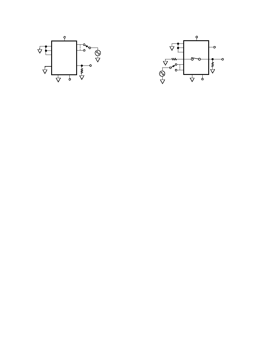
REV. A
–10–
ADG608/ADG609
A2
VOUT
VSS
VDD
D
A1
A0
EN
GND
ADG608
RL
1k
VSS
VDD
S1
VS
S2
S8
2.4V
1k
Test Circuit 10. Channel-to-Channel Crosstalk
A2
VOUT
VSS
VDD
D
A1
A0
EN
GND
ADG608
RL
1k
VSS
VDD
S1
VS
S8
Test Circuit 9. OFF Isolation
TERMINOLOGY
VDD
Most positive power supply potential.
VSS
Most negative power supply potential in dual
supplies. In single supply applications, it may
be connected to ground.
GND
Ground (0 V) reference.
RON
Ohmic resistance between D and S.
R
ON
RON variation due to a change in the analog
input voltage with a constant load current.
RON Match
Difference between the RON of any two
channels.
IS (OFF)
Source leakage current when the switch is off.
ID (OFF)
Drain leakage current when the switch is off.
ID, IS (ON)
Channel leakage current when the switch is
on.
VD, VS
Analog voltage on terminals D, S.
CS (OFF)
Channel input capacitance for “OFF”
condition.
CD (OFF)
Channel output capacitance for “OFF”
condition.
CD, CS (ON)
“ON” switch capacitance.
CIN
Digital input capacitance.
tON (EN)
Delay time between the 50% and 90% points
of the digital input and switch “ON”
condition.
tOFF (EN)
Delay time between the 50% and 90% points
of the digital input and switch “OFF”
condition.
tTRANSITION
Delay time between the 50% and 90% points
of the digital inputs and the switch “ON”
condition when switching from one address
state to another.
tOPEN
“OFF” time measured between the 80%
points of both switches when switching from
one address state to another.
VINL
Maximum input voltage for logic “0.”
VINH
Minimum input voltage for logic “1.”
IINL (IINH)
Input current of the digital input.
Crosstalk
A measure of unwanted signal which is
coupled through from one channel to another
as a result of parasitic capacitance.
Off Isolation
A measure of unwanted signal coupling
through an “OFF” channel.
Charge Injection A measure of the glitch impulse transferred
from the digital input to the analog output
during switching.
IDD
Positive supply current.
ISS
Negative supply current.
相关PDF资料 |
PDF描述 |
|---|---|
| VE-B61-CU-F4 | CONVERTER MOD DC/DC 12V 200W |
| LTC201ACS#PBF | IC SWITCH QUAD SPST 16SOIC |
| PIC16CE624-04I/SS | IC MCU OTP 1KX14 EE COMP 20SSOP |
| VE-B61-CU-F3 | CONVERTER MOD DC/DC 12V 200W |
| ADG1211YRUZ | IC SWITCH QUAD SPST 16TSSOP |
相关代理商/技术参数 |
参数描述 |
|---|---|
| ADG608BR | 功能描述:IC MULTIPLEXER 8X1 16SOIC RoHS:否 类别:集成电路 (IC) >> 接口 - 模拟开关,多路复用器,多路分解器 系列:- 其它有关文件:STG4159 View All Specifications 标准包装:5,000 系列:- 功能:开关 电路:1 x SPDT 导通状态电阻:300 毫欧 电压电源:双电源 电压 - 电源,单路/双路(±):±1.65 V ~ 4.8 V 电流 - 电源:50nA 工作温度:-40°C ~ 85°C 安装类型:表面贴装 封装/外壳:7-WFBGA,FCBGA 供应商设备封装:7-覆晶 包装:带卷 (TR) |
| ADG608BR-REEL | 功能描述:IC MULTIPLEXER 8X1 16SOIC RoHS:否 类别:集成电路 (IC) >> 接口 - 模拟开关,多路复用器,多路分解器 系列:- 标准包装:1,000 系列:- 功能:多路复用器 电路:1 x 4:1 导通状态电阻:- 电压电源:双电源 电压 - 电源,单路/双路(±):±5V 电流 - 电源:7mA 工作温度:-40°C ~ 85°C 安装类型:表面贴装 封装/外壳:16-SOIC(0.154",3.90mm 宽) 供应商设备封装:16-SOIC 包装:带卷 (TR) |
| ADG608BR-REEL7 | 制造商:Analog Devices 功能描述:5V/3V 8CH/4 DIFF,CH.MUX. I.C. - Tape and Reel |
| ADG608BRU | 功能描述:IC MULTIPLEXER 8X1 16TSSOP RoHS:否 类别:集成电路 (IC) >> 接口 - 模拟开关,多路复用器,多路分解器 系列:- 其它有关文件:STG4159 View All Specifications 标准包装:5,000 系列:- 功能:开关 电路:1 x SPDT 导通状态电阻:300 毫欧 电压电源:双电源 电压 - 电源,单路/双路(±):±1.65 V ~ 4.8 V 电流 - 电源:50nA 工作温度:-40°C ~ 85°C 安装类型:表面贴装 封装/外壳:7-WFBGA,FCBGA 供应商设备封装:7-覆晶 包装:带卷 (TR) |
| ADG608BRU-REEL7 | 功能描述:IC MULTIPLEXER 8X1 16TSSOP RoHS:否 类别:集成电路 (IC) >> 接口 - 模拟开关,多路复用器,多路分解器 系列:- 标准包装:1,000 系列:- 功能:多路复用器 电路:1 x 4:1 导通状态电阻:- 电压电源:双电源 电压 - 电源,单路/双路(±):±5V 电流 - 电源:7mA 工作温度:-40°C ~ 85°C 安装类型:表面贴装 封装/外壳:16-SOIC(0.154",3.90mm 宽) 供应商设备封装:16-SOIC 包装:带卷 (TR) |
发布紧急采购,3分钟左右您将得到回复。