- 您现在的位置:买卖IC网 > PDF目录11485 > ADG715BRUZ (Analog Devices Inc)IC SWITCH OCTAL SPST 24TSSOP PDF资料下载
参数资料
| 型号: | ADG715BRUZ |
| 厂商: | Analog Devices Inc |
| 文件页数: | 5/16页 |
| 文件大小: | 0K |
| 描述: | IC SWITCH OCTAL SPST 24TSSOP |
| 产品培训模块: | iCMOS™ Switches and Multiplexers for Data Acquisition Switch Fundamentals |
| 标准包装: | 62 |
| 功能: | 开关 |
| 电路: | 8 x SPST - NO |
| 导通状态电阻: | 4.5 欧姆 |
| 电压电源: | 单/双电源 |
| 电压 - 电源,单路/双路(±): | 2.7 V ~ 5.5 V,±2.5V |
| 电流 - 电源: | 10µA |
| 工作温度: | -40°C ~ 85°C |
| 安装类型: | 表面贴装 |
| 封装/外壳: | 24-TSSOP(0.173",4.40mm 宽) |
| 供应商设备封装: | 24-TSSOP |
| 包装: | 管件 |
| 产品目录页面: | 803 (CN2011-ZH PDF) |
ADG714/ADG715
–13–
REV.
A repeated write function gives the user flexibility to update the
matrix switch a number of times after addressing the part only
once. During the write cycle, each data byte will update the con-
guration of the switches. For example, after the matrix switch
has acknowledged its address byte, and received one data byte,
the switches will update after the data byte; if another data byte
is written to the matrix switch while it is still the addressed slave
device, this data byte will also cause a switch conguration update.
Repeat read of the matrix switch is also allowed.
Input Shift Register
The input shift register is eight bits wide. Figure 3 illustrates
the contents of the input shift register. Data is loaded into the
device as an 8-bit word under the control of a serial clock input,
SCL. The timing diagram for this operation is shown in Figure
2. The 8-bit word consists of eight data bits, each controlling
one switch. MSB (Bit 7) is loaded rst.
Write Operation
When writing to the ADG715, the user must begin with an address
byte and R/
W bit, after which the switch will acknowledge that
it is prepared to receive data by pulling SDA low. This address
byte is followed by the 8-bit word. The write operation for the
switch is shown in the Figure 4.
READ Operation
When reading data back from the ADG715, the user must begin
with an address byte and R/
W bit, after which the switch will
acknowledge that it is prepared to transmit data by pulling SDA
low. The readback operation is a single byte that consists of the
eight data bits in the input register. The read operation for the
part is shown in Figure 5.
SCL
SDA
S8
S7
S6
S5
S4
S3
S2
S1
0
1
0
A0
R/W
STOP
COND
BY
MASTER
ACK
BY
ADG715
START
COND
BY
MASTER
ADDRESS BYTE
DATA BYTE
ACK
BY
ADG715
A1
1
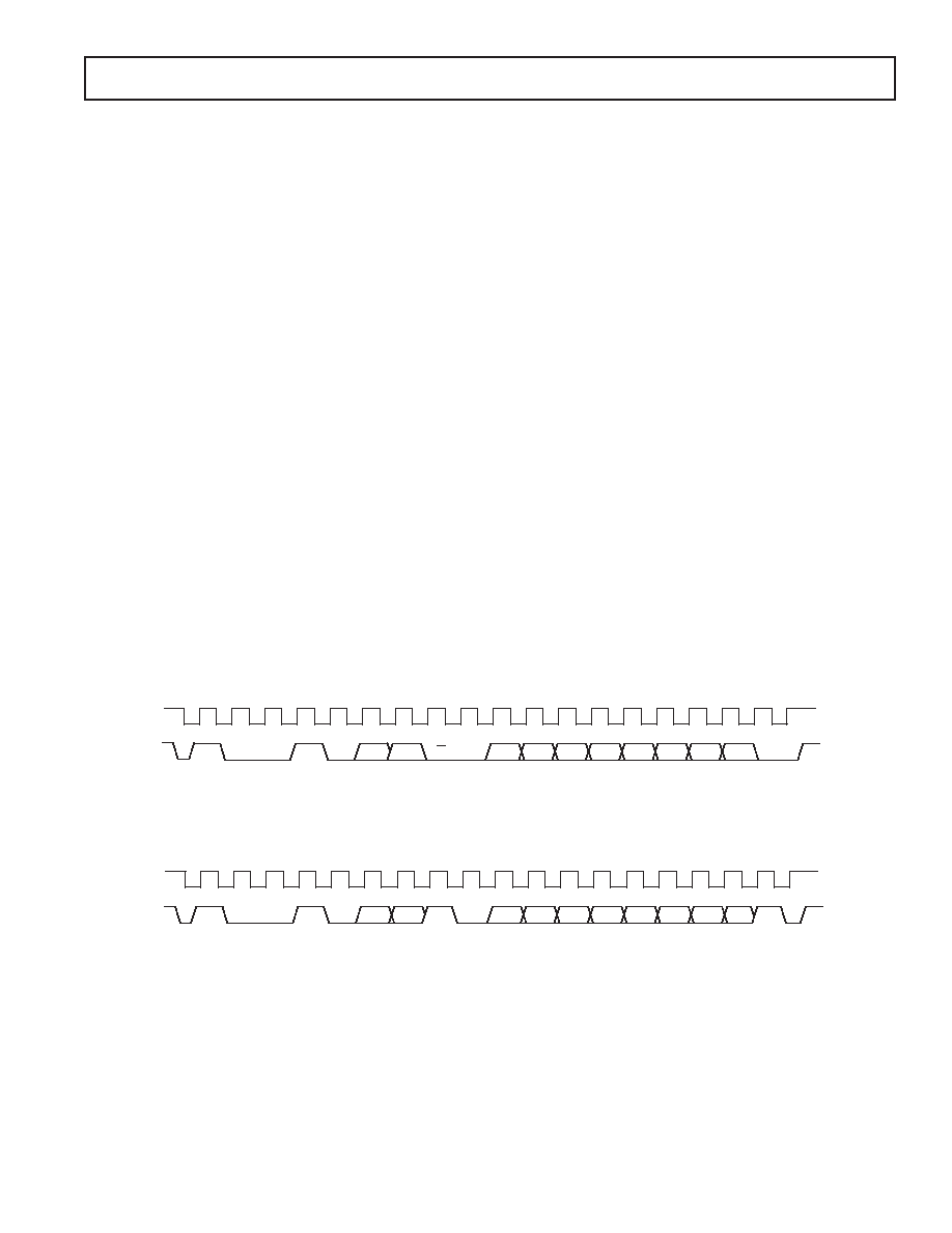
Figure 4. ADG715 Write Sequence
SCL
SDA
S8
S7
S6
S5
S4
S3
S2
S1
0
1
0
A0
R/
W
STOP
COND
BY
MASTER
ACK
BY
ADG715
START
COND
BY
MASTER
ADDRESS BYTE
DATA BYTE
NO ACK
BY
MASTER
A1
1
Figure 5. ADG715 Readback Sequence
The 2-wire serial bus protocol operates as follows:
1. The master initiates data transfer by establishing a START
condition, which is when a high-to-low transition on the
SDA line occurs while SCL is high. The following byte is the
address byte that consists of the 7-bit slave address followed
by a R/
W bit (this bit determines whether data will be read
from or written to the slave device).
The slave whose address corresponds to the transmitted address
responds by pulling the SDA line low during the ninth clock
pulse (this is termed the acknowledge bit). At this stage,
all other devices on the bus remain idle while the selected
device waits for data to be written to or read from its serial
register. If the R/
W bit is high, the master will read from the
slave device. However, if the R/
W bit is low, the master will
write to the slave device.
2. Data is transmitted over the serial bus in sequences of nine
clock pulses (eight data bits followed by an acknowledge bit).
The transitions on the SDA line must occur during the
low period of SCL and remain stable during the high
period of SCL.
3. When all data bits have been read or written, a STOP con-
dition is established by the master. A STOP condition is
dened as a low-to-high transition on the SDA line while
SCL is high. In write mode, the master will pull the SDA
line high during the tenth clock pulse to establish a STOP
condition. In read mode, the master will issue a no acknowledge
for the ninth clock pulse (i.e., the SDA line remains high).
The master will then bring the SDA line low before the tenth
clock pulse and then high during the tenth clock pulse to estab-
lish a STOP condition.
See Figure 4 for a graphical explanation of the serial interface.
C
相关PDF资料 |
PDF描述 |
|---|---|
| VE-B6Y-IW-B1 | CONVERTER MOD DC/DC 3.3V 66W |
| VE-B6F-IY-B1 | CONVERTER MOD DC/DC 72V 50W |
| VE-B63-IY-B1 | CONVERTER MOD DC/DC 24V 50W |
| GRM319R71C224KA01D | CAP CER 0.22UF 16V 10% X7R 1206 |
| GRM31MR72A823KA01L | CAP CER 0.082UF 100V X7R 1206 |
相关代理商/技术参数 |
参数描述 |
|---|---|
| ADG715BRUZ-REEL | 功能描述:IC SWITCH OCTAL SPST 24TSSOP RoHS:是 类别:集成电路 (IC) >> 接口 - 模拟开关,多路复用器,多路分解器 系列:- 标准包装:1,000 系列:- 功能:多路复用器 电路:1 x 4:1 导通状态电阻:- 电压电源:双电源 电压 - 电源,单路/双路(±):±5V 电流 - 电源:7mA 工作温度:-40°C ~ 85°C 安装类型:表面贴装 封装/外壳:16-SOIC(0.154",3.90mm 宽) 供应商设备封装:16-SOIC 包装:带卷 (TR) |
| ADG715BRUZ-REEL7 | 功能描述:IC SWITCH OCTAL SPST 24TSSOP RoHS:是 类别:集成电路 (IC) >> 接口 - 模拟开关,多路复用器,多路分解器 系列:- 标准包装:1,000 系列:- 功能:多路复用器 电路:1 x 4:1 导通状态电阻:- 电压电源:双电源 电压 - 电源,单路/双路(±):±5V 电流 - 电源:7mA 工作温度:-40°C ~ 85°C 安装类型:表面贴装 封装/外壳:16-SOIC(0.154",3.90mm 宽) 供应商设备封装:16-SOIC 包装:带卷 (TR) |
| ADG719 | 制造商:AD 制造商全称:Analog Devices 功能描述:CMOS Low Voltage 4 ohm SPDT Switch |
| ADG719_10 | 制造商:AD 制造商全称:Analog Devices 功能描述:CMOS 1.8 V to 5.5 V, 2.5 ?? 2:1 Mux/SPDT Switch in SOT-23 |
| ADG719BRM | 功能描述:IC SWITCH SPDT 8MSOP RoHS:否 类别:集成电路 (IC) >> 接口 - 模拟开关,多路复用器,多路分解器 系列:- 标准包装:1,000 系列:- 功能:多路复用器 电路:1 x 4:1 导通状态电阻:- 电压电源:双电源 电压 - 电源,单路/双路(±):±5V 电流 - 电源:7mA 工作温度:-40°C ~ 85°C 安装类型:表面贴装 封装/外壳:16-SOIC(0.154",3.90mm 宽) 供应商设备封装:16-SOIC 包装:带卷 (TR) |
发布紧急采购,3分钟左右您将得到回复。