- 您现在的位置:买卖IC网 > PDF目录11252 > ADG819BRTZ-REEL7 (Analog Devices Inc)IC SWITCH SPDT SOT23-6 PDF资料下载
参数资料
| 型号: | ADG819BRTZ-REEL7 |
| 厂商: | Analog Devices Inc |
| 文件页数: | 1/12页 |
| 文件大小: | 0K |
| 描述: | IC SWITCH SPDT SOT23-6 |
| 产品培训模块: | Switch Fundamentals |
| 标准包装: | 3,000 |
| 功能: | 开关 |
| 电路: | 1 x SPDT - NC/NO |
| 导通状态电阻: | 600 毫欧 |
| 电压电源: | 单电源 |
| 电压 - 电源,单路/双路(±): | 1.8 V ~ 5.5 V |
| 电流 - 电源: | 1nA |
| 工作温度: | -40°C ~ 125°C |
| 安装类型: | 表面贴装 |
| 封装/外壳: | SOT-23-6 |
| 供应商设备封装: | SOT-23-6 |
| 包装: | 带卷 (TR) |
0.5
n CMOS
a
1.8 V to 5.5 V 2:1 Mux/SPDT Switches
FEATURES
Low On Resistance 0.8
n Max at 125°C
0.25
n Max On Resistance Flatness
1.8 V to 5.5 V Single Supply
200 mA Current Carrying Capability
Automotive Temperature Range: –40
°C to +125°C
Rail-to-Rail Operation
6-Lead SOT-23 Package, 8-Lead
/SOIC Package, and
6-Bump MicroCSP (Micro Chip Scale Package) ADG819
Fast Switching Times
Typical Power Consumption (<0.01
/W)
TTL-/CMOS-Compatible Inputs
Pin Compatible with the ADG719 (ADG819)
APPLICATIONS
Power Routing
Battery-Powered Systems
Communication Systems
Data Acquisition Systems
Cellular Phones
Modems
PCMCIA Cards
Hard Drives
Relay Replacement
GENERAL DESCRIPTION
The ADG819 and the ADG820 are monolithic, CMOS, SPDT
(single-pole, double-throw) switches. These switches are designed
on a submicron process that provides low power dissipation yet
gives high switching speed, low On resistance, and low leakage
currents.
Low power consumption and an operating supply range of 1.8 V
to 5.5 V make the ADG819 and ADG820 ideal for battery-pow
ered, portable instruments.
Each switch of the ADG819 and the ADG820 conducts equally
well in both directions when on. The ADG819 exhibits break
before-make switching action, thus preventing momentary shorting
when switching channels. The ADG820 exhibits make-before
break action.
The ADG819 and the ADG820 are available in a 6-lead SOT-23
package and an 8-lead
SOIC package. The ADG819 is also
available in a 2
× 3 bump 1.14 mm × 2.18 mm MicroCSP
package. This chip occupies only a 1.14 mm
× 2.18 mm area,
making it the ideal candidate for space-constrained applications.
REV. 0
Information furnished by Analog Devices is believed to be accurate and
reliable. However, no responsibility is assumed by Analog Devices for its
use, nor for any infringements of patents or other rights of third parties that
may result from its use. No license is granted by implication or otherwise
under any patent or patent rights of Analog Devices.
ADG819/ADG820
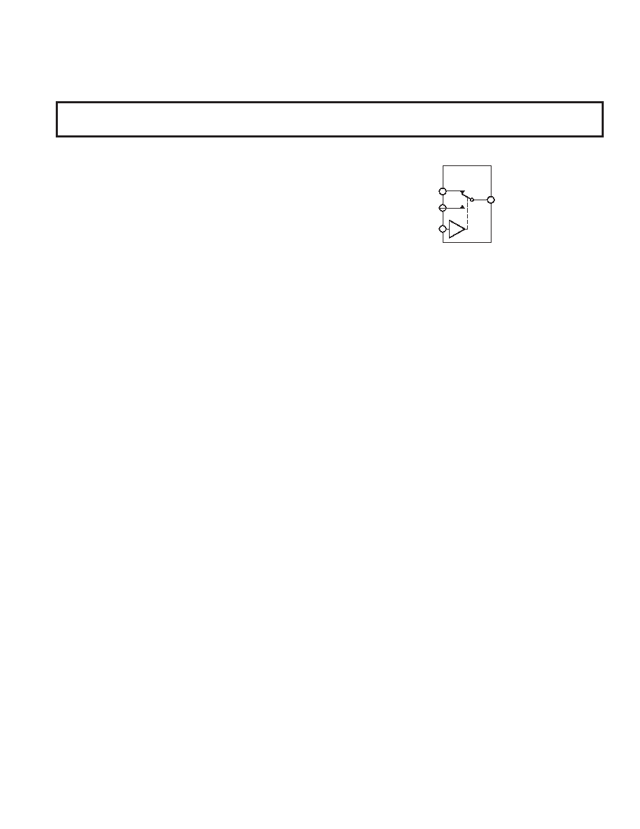
FUNCTIONAL BLOCK DIAGRAM
S2
D
S1
IN
ADG819/
ADG820
SWITCHES SHOWN
FOR A LOGIC “1” INPUT
PRODUCT HIGHLIGHTS
1. Very low ON resistance, 0.5
typical
2. 1.8 V to 5.5 V single-supply operation
3. High current carrying capability
4. Tiny 6-lead SOT-23 package, 8-lead
SOIC package,
and 2
× 3 bump 1.14 mm × 2.18 mm MicroCSP package
(ADG819 only)
One Technology Way, P.O. Box 9106, Norwood, MA 02062-9106, U.S.A.
Tel: 781/329-4700
Fax: 781/326-8703
Analog Devices, Inc., 2002
相关PDF资料 |
PDF描述 |
|---|---|
| GRM31M6T1H332JD01L | CAP CER 3300PF 50V 5% T2H 1206 |
| DEA1X3F100JCDB | CAP CER 10PF 3.15KV 5% RADIAL |
| ADG633YCPZ-REEL7 | IC SWITCH TRIPLE SPDT 16LFCSP |
| RPER71H223K2K1A03B | CAP CER 0.022UF 50V 10% RADIAL |
| CDR31BX103AMUS | CAP CER 10000PF 50V 20% BX 0805 |
相关代理商/技术参数 |
参数描述 |
|---|---|
| ADG820 | 制造商:AD 制造商全称:Analog Devices 功能描述:0.5 OHM CMOS 1.8 V to 5.5 V 2:1 Mux/SPDT Switches |
| ADG820BRM | 制造商:Rochester Electronics LLC 功能描述:SPDT (MBB) - Bulk 制造商:Analog Devices 功能描述: |
| ADG820BRM-REEL | 制造商:Analog Devices 功能描述:Analog Switch Single SPDT 8-Pin MSOP T/R |
| ADG820BRM-REEL7 | 制造商:Analog Devices 功能描述:Analog Switch Single SPDT 8-Pin MSOP T/R 制造商:Rochester Electronics LLC 功能描述:SPDT (MBB) - Tape and Reel |
| adg820brmz | 制造商:Rochester Electronics LLC 功能描述: 制造商:Analog Devices 功能描述: |
发布紧急采购,3分钟左右您将得到回复。