- 您现在的位置:买卖IC网 > PDF目录11248 > ADG836YRMZ-REEL7 (Analog Devices Inc)IC SWITCH DUAL SPDT 10MSOP PDF资料下载
参数资料
| 型号: | ADG836YRMZ-REEL7 |
| 厂商: | Analog Devices Inc |
| 文件页数: | 14/16页 |
| 文件大小: | 0K |
| 描述: | IC SWITCH DUAL SPDT 10MSOP |
| 产品培训模块: | Switch Fundamentals |
| 标准包装: | 1,000 |
| 功能: | 开关 |
| 电路: | 2 x SPDT - NC/NO |
| 导通状态电阻: | 650 毫欧 |
| 电压电源: | 单电源 |
| 电压 - 电源,单路/双路(±): | 1.65 V ~ 3.6 V |
| 电流 - 电源: | 3nA |
| 工作温度: | -40°C ~ 125°C |
| 安装类型: | 表面贴装 |
| 封装/外壳: | 10-TFSOP,10-MSOP(0.118",3.00mm 宽) |
| 供应商设备封装: | 10-MSOP |
| 包装: | 带卷 (TR) |
ADG836
Rev. A | Page 7 of 16
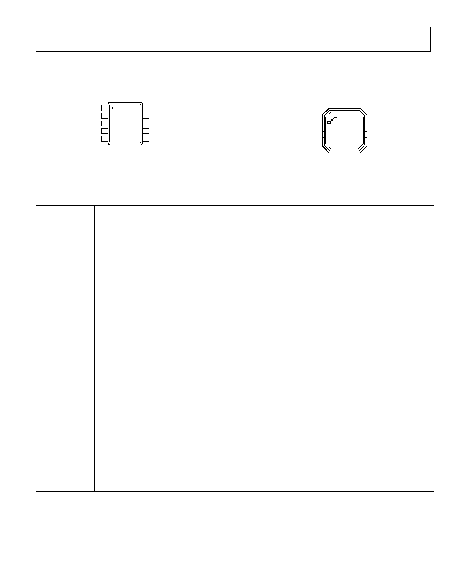
PIN CONFIGURATIONS
IN1
1
S1A
2
GND
3
S2A
4
IN2
5
D1
10
S1B
9
VDD
8
S2B
7
D2
6
ADG836
TOP VIEW
(Not to Scale)
04308-002
Figure 2. 10-Lead MSOP (RM-10)
PIN 1
INDICATOR
NC = NO CONNECT
1
S1A
2
GND
3
S2A
9 S1B
8VDD
7 S2B
4
N
C
5
IN
2
6
D
2
1
2
N
C
1
N
1
0
D
1
TOP VIEW
(Not to Scale)
ADG836
04308-003
Figure 3. 12-Lead LFCSP (CP-12)
Table 6. Terminology
VDD
Most positive power supply potential.
IDD
Positive supply current.
GND
Ground (0 V) reference.
S
Source terminal. May be an input or output.
D
Drain terminal. May be an input or output.
IN
Logic control input.
VD (VS)
Analog voltage on terminals D, S.
RON
Ohmic resistance between D and S.
RFLAT (ON)
Flatness is defined as the difference between the maximum and minimum value of on resistance as measured over the
specified analog signal range.
RON
On resistance match between any two channels.
IS (OFF)
Source leakage current with the switch off.
ID (OFF)
Drain leakage current with the switch off.
ID, IS (ON)
Channel leakage current with the switch on.
VINL
Maximum input voltage for Logic 0.
VINH
Minimum input voltage for Logic 1.
IINL (IINH)
Input current of the digital input.
CS (OFF)
Off switch source capacitance. Measured with reference to ground.
CD (OFF)
Off switch drain capacitance. Measured with reference to ground.
CD, CS (ON)
On switch capacitance. Measured with reference to ground.
CIN
Digital input capacitance.
tON
Delay time between the 50% and the 90% points of the digital input and switch on condition.
tOFF
Delay time between the 50% and the 90% points of the digital input and switch off condition.
tBBM
On or off time measured between the 80% points of both switches when switching from one to another.
Charge Injection
A measure of the glitch impulse transferred from the digital input to the analog output during on-off switching.
Off Isolation
A measure of unwanted signal coupling through an off switch.
Crosstalk
A measure of unwanted signal, which is coupled through from one channel to another, as a result of parasitic
capacitance.
3 dB Bandwidth
The frequency at which the output is attenuated by 3 dB.
On Response
The frequency response of the on switch.
Insertion Loss
The loss due to the on resistance of the switch.
THD + N
The ratio of the harmonics amplitude plus noise of a signal to the fundamental.
相关PDF资料 |
PDF描述 |
|---|---|
| ADG804YRMZ-REEL7 | IC MULTIPLEXER 4X1 10MSOP |
| VE-JWW-IX-F4 | CONVERTER MOD DC/DC 5.5V 75W |
| ADG719BRTZ-500RL7 | IC SWITCH SPDT SOT23-6 |
| VE-JWV-IX-F3 | CONVERTER MOD DC/DC 5.8V 75W |
| VE-JWT-IX-F2 | CONVERTER MOD DC/DC 6.5V 75W |
相关代理商/技术参数 |
参数描述 |
|---|---|
| ADG839 | 制造商:AD 制造商全称:Analog Devices 功能描述:0.35 ohm CMOS 1.65 V to 3.6 V Single SPDT Switch/2:1 MUX |
| ADG839YKSZ-500RL7 | 功能描述:IC SWITCH SPDT SC70-6 RoHS:是 类别:集成电路 (IC) >> 接口 - 模拟开关,多路复用器,多路分解器 系列:- 应用说明:Ultrasound Imaging Systems Application Note 产品培训模块:Lead (SnPb) Finish for COTS Obsolescence Mitigation Program 标准包装:250 系列:- 功能:开关 电路:单刀单掷 导通状态电阻:48 欧姆 电压电源:单电源 电压 - 电源,单路/双路(±):2.7 V ~ 5.5 V 电流 - 电源:5µA 工作温度:0°C ~ 70°C 安装类型:表面贴装 封装/外壳:48-LQFP 供应商设备封装:48-LQFP(7x7) 包装:托盘 |
| ADG839YKSZ-REEL | 功能描述:IC SWITCH SPDT SC70-6 RoHS:是 类别:集成电路 (IC) >> 接口 - 模拟开关,多路复用器,多路分解器 系列:- 标准包装:1,000 系列:- 功能:多路复用器 电路:1 x 4:1 导通状态电阻:- 电压电源:双电源 电压 - 电源,单路/双路(±):±5V 电流 - 电源:7mA 工作温度:-40°C ~ 85°C 安装类型:表面贴装 封装/外壳:16-SOIC(0.154",3.90mm 宽) 供应商设备封装:16-SOIC 包装:带卷 (TR) |
| ADG839YKSZ-REEL7 | 功能描述:IC SWITCH SPDT SC70-6 RoHS:是 类别:集成电路 (IC) >> 接口 - 模拟开关,多路复用器,多路分解器 系列:- 标准包装:1,000 系列:- 功能:多路复用器 电路:1 x 4:1 导通状态电阻:- 电压电源:双电源 电压 - 电源,单路/双路(±):±5V 电流 - 电源:7mA 工作温度:-40°C ~ 85°C 安装类型:表面贴装 封装/外壳:16-SOIC(0.154",3.90mm 宽) 供应商设备封装:16-SOIC 包装:带卷 (TR) |
| ADG841 | 制造商:AD 制造商全称:Analog Devices 功能描述:0.28 OHM CMOS 1.65 V to 3.6 V Single SPST Switches in SC70 |
发布紧急采购,3分钟左右您将得到回复。