参数资料
| 型号: | ADL5315-EVAL |
| 厂商: | Analog Devices Inc |
| 文件页数: | 14/20页 |
| 文件大小: | 0K |
| 描述: | BOARD EVAL FOR ADL5315 |
| 设计资源: | Interfacing ADL5315 to Translinear Logarithmic Amplifier (CN0056) |
| 标准包装: | 1 |
| 主要目的: | 电源管理,电流镜像 |
| 嵌入式: | 否 |
| 已用 IC / 零件: | ADL5315 |
| 主要属性: | 电流镜像,高端,3nA ~ 3mA |
| 次要属性: | 2.7 ~ 8 V 1% 线性可调式输入电流限制 |
| 已供物品: | 板 |
| 相关产品: | ADL5315ACPZ-R7DKR-ND - IC CURRENT MONITOR 8LFCSP ADL5315ACPZ-R7CT-ND - IC CURRENT MONITOR 8LFCSP ADL5315ACPZ-R7TR-ND - IC CURRENT MONITOR 8LFCSP |
�� �
�
�ADL5315�
�2.2�
�2.0�
�1.8�
�1.6�
�1.4�
�1.2�
�1.0�
�0.8�
�0.6�
�0.4�
�0.2�
�CHARACTERIZATION� METHODS�
�During� characterization,� the� ADL5315� was� treated� as� a�
�precision� 1:1� current� mirror.� To� make� accurate� measurements�
�throughout� the� six-decade� current� range,� calibrated� Keithley�
�236� current� sources� were� used� to� create� and� measure� the� test�
�currents.� Measurements� at� low� currents� are� very� susceptible� to�
�leakage� to� the� ground� plane.� To� minimize� leakage� on� the�
�characterization� board,� the� VSET� pin� is� connected� to� traces� that�
�buffer� V� INPT� from� ground.� These� traces� are� connected� to� the�
�triax� guard� connector� to� provide� buffering� along� the� cabling.�
�0�
�100p�
�1n�
�10n�
�100n�
�1� μ�
�10� μ�
�100� μ�
�1m�
�10m�
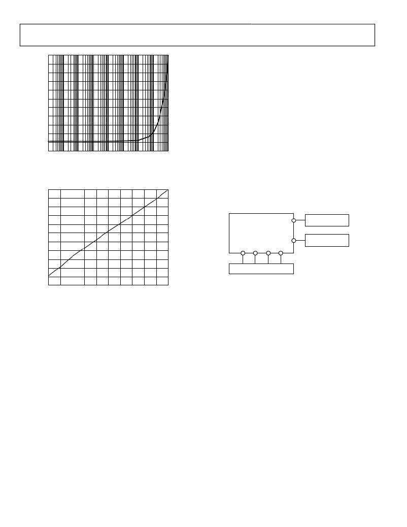
�The� primary� characterization� setup� shown� in� Figure� 30� is� used�
�to� perform� all� static� measurements,� including� mirror� linearity�
�2.2�
�2.0�
�1.8�
�1.6�
�I� INPT� (A)�
�Figure� 28.� V� SET� Voltage� vs.� I� INPT� when�
�RLIM� Is� Configured� for� Automatic� Photodiode� Biasing�
�between� I� INPT� and� I� OUT� ,� V� INPT� variation� vs.� I� INPT� ,� supply� current,� and�
�I� INPT� current� limiting.� Component� selection� of� the� characterization�
�board� is� similar� to� that� of� the� evaluation� board,� except� that� triax�
�connectors� are� used� instead� of� SMA.� To� measure� pulse� response,�
�noise,� and� small� signal� bandwidth,� more� specialized� test� setups�
�are� used.�
�1.4�
�ADL5315�
�INPT�
�KEITHLEY� 236�
�1.2�
�CHARACTERIZATION� BOARD�
�1.0�
�0.8�
�0.6�
�IOUT�
�VPOS� VSET� SREF� COMM�
�KEITHLEY� 236�
�0.4�
�0.2�
�0�
�DC� SUPPLIES/DMM�
�Figure� 30.� Primary� Characterization� Setup�
�0� 1� 2� 3� 4� 5� 6� 7� 8� 9�
�I� INPT� (mA)�
�Figure� 29.� V� SET� Voltage� vs.� I� INPT� when�
�RLIM� Is� Configured� for� Automatic� Photodiode� Biasing�
�10�
�The� setup� in� Figure� 31� is� used� to� measure� the� output� current�
�noise� of� the� ADL5315.� Batteries� are� used� in� numerous� places� to�
�minimize� introduced� noise� and� remove� the� uncertainty�
�resulting� from� the� use� of� multiple� dc� supplies.� In� application,�
���low� value� for� small� input� currents� to� minimize� dark� current.�
�The� V� SET� voltage� increases� in� a� linear� manner� at� the� higher� input�
�currents� to� maintain� accurate� photodiode� responsivity.� The�
�minimum� bias� level� for� the� configuration� above� is� ~200� mV.�
�properly� bypassed� dc� supplies� provide� similar� results.� The� load�
�resistor� is� chosen� for� each� current� to� maximize� signal-to-noise�
�ratio� while� maintaining� measurement� system� bandwidth� (when�
�combined� with� the� low� capacitance� JFET� buffer).� The� custom�
�LNA� is� used� to� overcome� noise� floor� limitations� in� the�
�HP89410A� signal� analyzer.�
�Rev.� 0� |� Page� 14� of� 20�
�相关PDF资料 |
PDF描述 |
|---|---|
| ADM00333 | BOARD EVAL FOR PIC18F87J72 |
| ADM00344 | BOARD DEMO EVAL FOR RE46C190 |
| ADM00345 | BOARD DEMO 3PH BLDC CTLR MTD6505 |
| ADM1026EBZEVB | BOARD EVAL FOR ADM1026 |
| ADN8831-EVALZ | BOARD EVAL FOR ADN8831 |
相关代理商/技术参数 |
参数描述 |
|---|---|
| ADL5317 | 制造商:AD 制造商全称:Analog Devices 功能描述:Avalanche Photodiode Bias Controller and Wide Range (5 nA to 5 mA) Current Monitor |
| ADL5317ACPZ-REEL7 | 功能描述:IC CURRENT MONITOR 16LFCSP RoHS:是 类别:集成电路 (IC) >> PMIC - 稳流/电流管理 系列:- 产品培训模块:Lead (SnPb) Finish for COTS Obsolescence Mitigation Program 标准包装:50 系列:- 功能:电流开关 检测方法:- 精确度:±10% 输入电压:1.7 V ~ 5.5 V 电流 - 输出:600mA 工作温度:-40°C ~ 125°C 安装类型:表面贴装 封装/外壳:10-UFQFN 供应商设备封装:10-UTQFN(1.4x1.8) 包装:管件 |
| ADL5317ACPZ-WP | 制造商:Analog Devices 功能描述:SP Amp LOG Amp Single 6V/80V 16-Pin LFCSP EP Tray 制造商:Analog Devices 功能描述:SP AMP LOG AMP SGL 6V/80V 16LFCSP EP - Bulk |
| ADL5317-EVAL | 制造商:Analog Devices 功能描述:EVAL BD FOR AVALANCHE PHOTODIODE BIAS CNTRLR AND WIDE RANGE - Bulk |
| ADL531A-53M0 | 制造商:Panasonic Industrial Company 功能描述:VALVE |
发布紧急采购,3分钟左右您将得到回复。