- 您现在的位置:买卖IC网 > PDF目录15791 > ADM1024EVB (ON Semiconductor)BOARD EVAL FOR ADM1024 PDF资料下载
参数资料
| 型号: | ADM1024EVB |
| 厂商: | ON Semiconductor |
| 文件页数: | 21/30页 |
| 文件大小: | 0K |
| 描述: | BOARD EVAL FOR ADM1024 |
| 标准包装: | 1 |
| 其它名称: | EVAL-ADM1024EB EVAL-ADM1024EB-ND |
第1页第2页第3页第4页第5页第6页第7页第8页第9页第10页第11页第12页第13页第14页第15页第16页第17页第18页第19页第20页当前第21页第22页第23页第24页第25页第26页第27页第28页第29页第30页
ADM1024
http://onsemi.com
28
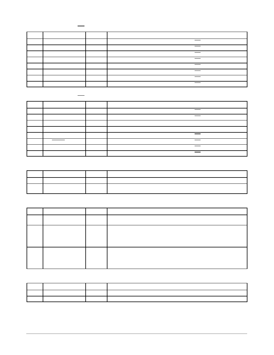
Table 16. REGISTER 43H, INT INTERRUPT MASK REGISTER 1 (POWER-ON DEFAULT, 00H)
Bit
Name
R/W
Description
0
2.5 V/Ext. Temp2
R/W
A 1 disables the corresponding interrupt status bit for INT interrupt.
1
VCCP1
R/W
A 1 disables the corresponding interrupt status bit for INT interrupt.
2
VCC
R/W
A 1 disables the corresponding interrupt status bit for INT interrupt.
3
5.0 V
R/W
A 1 disables the corresponding interrupt status bit for INT interrupt.
4
Int. Temp
R/W
A 1 disables the corresponding interrupt status bit for INT interrupt.
5
Ext. Temp1
R/W
A 1 disables the corresponding interrupt status bit for INT interrupt.
6
FAN1/AIN1
R/W
A 1 disables the corresponding interrupt status bit for INT interrupt.
7
FAN2/AIN2
R/W
A 1 disables the corresponding interrupt status bit for INT interrupt.
Table 17. REGISTER 44H, INT INTERRUPT MASK REGISTER 2 (POWER-ON DEFAULT, 00H)
Bit
Name
R/W
Description
0
12 V
R/W
A 1 disables the corresponding interrupt status bit for INT interrupt.
1
VCCP2
R/W
A 1 disables the corresponding interrupt status bit for INT interrupt.
2
Reserved
R/W
Powerup Default Set to Low.
3
Reserved
R/W
Powerup Default Set to Low.
4
CI
R/W
A 1 disables the corresponding interrupt status bit for INT interrupt.
5
THERM (Input)
R/W
A 1 disables the corresponding interrupt status bit for INT interrupt.
6
D1 Fault
R/W
A 1 disables the corresponding interrupt status bit for INT interrupt.
7
D2 Fault
R/W
A 1 disables the corresponding interrupt status bit for INT interrupt.
Table 18. REGISTER 46H, CHASSIS INTRUSION CLEAR (POWER-ON DEFAULT, 00H)
Bit
Name
R/W
Description
0–6
Reserved
Read only
Undefined, always reads as 00h.
7
Chassis Int. Clear
R/W
A 1 outputs a minimum 20 ms active low pulse on the Chassis Intrusion pin. The
register bit clears itself after the pulse has been output.
Table 19. REGISTER 47H, VID03/FAN DIVISOR REGISTER (POWER-ON DEFAULT, 0101(VID30))
Bit
Name
R/W
Description
0–3
VID
Read only
The VID<3:0> inputs from processor core power supplies to indicate the operating
voltage (e.g., 1.3 V to 3.5 V).
4–5
FAN1 Divisor
R/W
Sets counter prescaler for FAN1 speed measurement.
<5:4> = 00 – divide by 1
<5:4> = 01 – divide by 2
<5:4> = 10 – divide by 4
<5:4> = 11 – divide by 8
6–7
FAN2 Divisor
R/W
Sets counter prescaler for FAN2 speed measurement.
<7:6> = 00 – divide by 1
<7:6> = 01 – divide by 2
<7:6> = 10 – divide by 4
<7:6> = 11 – divide by 8
Table 20. REGISTER 49H, VID4/DEVICE ID REGISTER (POWER-ON DEFAULT, 1000000(VID4))
Bit
Name
R/W
Description
0
VID4
Read only
VID4 Input from Pentium
1–7
Reserved
Read only
Undefined, always reads as 1000 000(VID4)
相关PDF资料 |
PDF描述 |
|---|---|
| ISC1210ERR82J | INDUCTOR WW 820NH 5% 1210 |
| ISC1210ERR68J | INDUCTOR WW 680NH 5% 1210 |
| ISC1210ERR56J | INDUCTOR WW 560NH 5% 1210 |
| MAX6439UTPSRD7+T | IC BATTERY MON SNGL SOT23-6 |
| MAX6439UTPSWD7+T | IC BATTERY MON SNGL SOT23-6 |
相关代理商/技术参数 |
参数描述 |
|---|---|
| ADM1025 | 制造商:AD 制造商全称:Analog Devices 功能描述:Low-Cost PC Hardware Monitor ASIC |
| ADM1025A | 制造商:AD 制造商全称:Analog Devices 功能描述:Low-Cost PC Hardware Monitor ASIC |
| ADM1025AARQ | 功能描述:IC MONITOR SYS/VOLT 5CH 16QSOP RoHS:否 类别:集成电路 (IC) >> 接口 - 专用 系列:- 标准包装:3,000 系列:- 应用:PDA,便携式音频/视频,智能电话 接口:I²C,2 线串口 电源电压:1.65 V ~ 3.6 V 封装/外壳:24-WQFN 裸露焊盘 供应商设备封装:24-QFN 裸露焊盘(4x4) 包装:带卷 (TR) 安装类型:表面贴装 产品目录页面:1015 (CN2011-ZH PDF) 其它名称:296-25223-2 |
| ADM1025AARQ-REEL | 制造商:Rochester Electronics LLC 功能描述:PC HARDWARE MONITOR I.C. - Tape and Reel |
| ADM1025AARQZ | 功能描述:IC MONITOR SYS/VOLT 5CH 16QSOP RoHS:是 类别:集成电路 (IC) >> 接口 - 专用 系列:- 标准包装:3,000 系列:- 应用:PDA,便携式音频/视频,智能电话 接口:I²C,2 线串口 电源电压:1.65 V ~ 3.6 V 封装/外壳:24-WQFN 裸露焊盘 供应商设备封装:24-QFN 裸露焊盘(4x4) 包装:带卷 (TR) 安装类型:表面贴装 产品目录页面:1015 (CN2011-ZH PDF) 其它名称:296-25223-2 |
发布紧急采购,3分钟左右您将得到回复。