- 您现在的位置:买卖IC网 > PDF目录16316 > ADM1064ASUZ (Analog Devices Inc)IC SEQUENCER/SUPERVISOR 48-TQFP PDF资料下载
参数资料
| 型号: | ADM1064ASUZ |
| 厂商: | Analog Devices Inc |
| 文件页数: | 18/32页 |
| 文件大小: | 0K |
| 描述: | IC SEQUENCER/SUPERVISOR 48-TQFP |
| 标准包装: | 1 |
| 系列: | Super Sequencer® |
| 类型: | 序列发生器 |
| 监视电压数目: | 10 |
| 输出: | 可编程 |
| 电压 - 阀值: | 可调节/可选择 |
| 工作温度: | -40°C ~ 85°C |
| 安装类型: | 表面贴装 |
| 封装/外壳: | 48-TQFP |
| 供应商设备封装: | 48-TQFP(7x7) |
| 包装: | 托盘 |
| 产品目录页面: | 788 (CN2011-ZH PDF) |
| 配用: | EVAL-ADM1064TQEB-ND - BOARD EVALUATION FOR ADM1064TQ |
第1页第2页第3页第4页第5页第6页第7页第8页第9页第10页第11页第12页第13页第14页第15页第16页第17页当前第18页第19页第20页第21页第22页第23页第24页第25页第26页第27页第28页第29页第30页第31页第32页
�� �
�
�ADM1064�
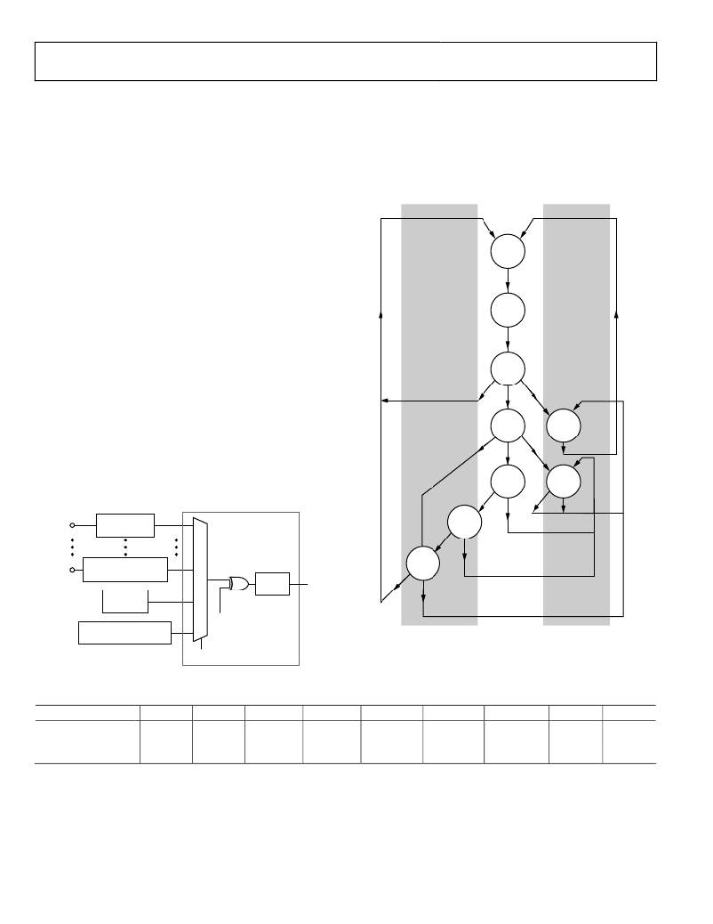
�SEQUENCING� ENGINE� APPLICATION� EXAMPLE�
�The� application� in� this� section� demonstrates� the� operation� of�
�the� SE.� Figure� 25� shows� how� the� simple� building� block� of� a� single�
�SE� state� can� be� used� to� build� a� power-up� sequence� for� a� three-�
�supply� system.� Table� 8� lists� the� PDOs� for� each� state� in� the� same� SE�
�implementation.� In� this� system,� a� good� 5� V� supply� on� VP1� and�
�the� VX1� pin� held� low� are� the� triggers� required� to� start� a� power-up�
�sequence.� The� sequence� next� turns� on� the� 3.3� V� supply,� then� the�
�2.5� V� supply� (assuming� successful� turn-on� of� the� 3.3� V� supply).�
�When� all� three� supplies� have� turned� on� correctly,� the� PWRGD�
�state� is� entered,� where� the� SE� remains� until� a� fault� occurs� on� one�
�of� the� three� supplies� or� until� it� is� instructed� to� go� through� a� power-�
�down� sequence� by� VX1� going� high.�
�Faults� are� dealt� with� throughout� the� power-up� sequence� on�
�a� case-by-case� basis.� The� following� three� sections� (the� Sequence�
�Detector� section,� the� Monitoring� Fault� Detector� section,� and�
�If� a� timer� delay� is� specified,� the� input� to� the� sequence� detector�
�must� remain� in� the� defined� state� for� the� duration� of� the� timer�
�delay.� If� the� input� changes� state� during� the� delay,� the� timer� is� reset.�
�The� sequence� detector� can� also� help� to� identify� monitoring� faults.�
�In� the� sample� application� shown� in� Figure� 25,� the� FSEL1� and�
�FSEL2� states� first� identify� which� of� the� VP1,VP2,� or� VP3� pins�
�has� faulted,� and� then� they� take� appropriate� action.�
�SEQUENCE�
�STATES�
�IDLE1�
�VX1� =� 0�
�IDLE2�
�the� Timeout� Detector� section)� describe� the� individual� blocks�
�and� use� the� sample� application� shown� in� Figure� 25� to� demonstrate�
�the� actions� of� the� state� machine.�
�Sequence� Detector�
�The� sequence� detector� block� is� used� to� detect� when� a� step� in�
�MONITOR� FAULT�
�STATES�
�VP1� =� 0�
�VP1� =� 1�
�EN3V3�
�10ms�
�VP2� =� 1�
�TIMEOUT�
�STATES�
�a� sequence� is� complete.� It� looks� for� one� of� the� SE� inputs� to�
�change� state� and� is� most� often� used� as� the� gate� for� successful�
�progress� through� a� power-up� or� power-down� sequence.� A� timer�
�(VP1� +� VP2)� =� 0�
�EN2V5�
�20ms�
�DIS3V3�
�VX1� =� 1�
�block� that� is� included� in� this� detector� can� insert� delays� into� a�
�power-up� or� power-down� sequence,� if� required.� Timer� delays�
�VP3� =� 1�
�can� be� set� from� 10� μs� to� 400� ms.� Figure� 24� is� a� block� diagram� of�
�the� sequence� detector.�
�(VP1� +� VP2� +� VP3)� =� 0�
�PWRGD�
�VP2� =� 0�
�DIS2V5�
�VX1� =� 1�
�VP1�
�VX5�
�SUPPLY� FAULT�
�DETECTION�
�LOGIC� INPUT� CHANGE�
�OR� FAULT� DETECTION�
�SEQUENCE�
�DETECTOR�
�VP1� =� 0�
�(VP1� +�
�VP2)� =� 0�
�FSEL2�
�FSEL1�
�VP3� =� 0�
�VX1� =� 1�
�TIMER�
�VP2� =� 0�
�WARNINGS�
�INVERT�
�FORCE� FLOW�
�(UNCONDITIONAL� JUMP)�
�SELECT�
�Figure� 24.� Sequence� Detector� Block� Diagram�
�Table� 8.� PDO� Outputs� for� Each� State�
�Figure� 25.� Sample� Application� Flow� Diagram�
�PDO� Outputs�
�PDO1� =� 3V3ON�
�PDO2� =� 2V5ON�
�PDO3� =� FAULT�
�IDLE1�
�0�
�0�
�0�
�IDLE2�
�0�
�0�
�0�
�EN3V3�
�1�
�0�
�0�
�EN2V5�
�1�
�1�
�0�
�DIS3V3�
�0�
�1�
�1�
�DIS2V5�
�1�
�0�
�1�
�PWRGD�
�1�
�1�
�0�
�FSEL1�
�1�
�1�
�1�
�FSEL2�
�1�
�1�
�1�
�Rev.� D� |� Page� 18� of� 32�
�相关PDF资料 |
PDF描述 |
|---|---|
| ECO-S2GB221CA | CAP ALUM 220UF 400V 20% SNAP |
| LTC690CN8#PBF | IC MPU SUPERVISORY CIRCUIT 8-DIP |
| M3DRK-1060K | IDC CABLE - MKR10K/MC10F/MPR10K |
| LTC2928IG#PBF | IC PWR SUPPLY SEQUENCER 36SSOP |
| 2-6278896-5 | CA,62.5,MTRJ-SC |
相关代理商/技术参数 |
参数描述 |
|---|---|
| ADM1065 | 制造商:AD 制造商全称:Analog Devices 功能描述:Super Sequencer-TM and Monitor |
| ADM1065ACP | 制造商:Analog Devices 功能描述:Volt Supervisor Sequencer/Monitor 2.7V to 5.4V 40-Pin LFCSP EP |
| ADM1065ACP-REEL | 制造商:AD 制造商全称:Analog Devices 功能描述:Super Sequencer-TM and Monitor |
| ADM1065ACP-REEL7 | 制造商:AD 制造商全称:Analog Devices 功能描述:Super Sequencer-TM and Monitor |
| ADM1065ACPZ | 功能描述:IC SEQUENCER/SUPERVISOR 40-LFCSP RoHS:是 类别:集成电路 (IC) >> PMIC - 监控器 系列:Super Sequencer® 标准包装:1 系列:- 类型:简单复位/加电复位 监视电压数目:1 输出:开路漏极或开路集电极 复位:高有效 复位超时:- 电压 - 阀值:1.8V 工作温度:-40°C ~ 125°C 安装类型:表面贴装 封装/外壳:6-TSOP(0.059",1.50mm 宽)5 引线 供应商设备封装:5-TSOP 包装:剪切带 (CT) 其它名称:NCP301HSN18T1GOSCT |
发布紧急采购,3分钟左右您将得到回复。